ASML “After Intel, TSMC, and others,
all EUV customers ordered the equipment”
Twice expensive thanexisting equipment,
dramatic rise in production for single patterning
Process competition likely to
Samsung Electronics and SK hynix placed an order for the next-generation semiconductor equipment 'High NA' extreme ultraviolet (EUV) exposure equipment to ASML. Following TSMC and Intel, Korean semiconductor manufacturers are also preparing to introduce equipment capable of realizing 2-nano process. The competition for the most advanced process is expected to intensify.
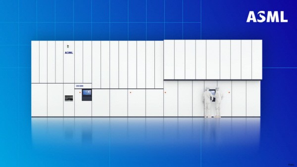
In an earnings announcement on the 19th, ASML said, "In the case of EUV high NA business, all EUV customers have placed orders for high NA products with additional orders for TWINSCAN EXE:5200 equipment." High NA EUV equipment is equipment that raises the lens numerical aperture (NA), which indicates the light collecting ability, from 0.33 to 0.55. It can process finer semiconductor circuits than existing EUV equipment. It is amajority opinionof industry that high NA equipment is essential for the 2-nanometer process.
Intel and TSMC have already officially announced the introduction of high NA EUV equipment. Intel announced that they were the first to place an order for high NA EUV equipment when they announced their strategy for an integrated semiconductor company (IDM 2.0) with the goal of re-entering the foundry market last year. This is to catch up with TSMC and Samsung Electronics' system semiconductor production capacity by preemptively introducing next-generation equipment. TSMC has also announced a contract to order high NA EUV equipment, but Samsung Electronics and SK hynix did not mention anything about the contract. With this ASML announcement, the introduction of high NA equipment by Korean semiconductor manufacturers has been officially formalized. However, Samsung Electronics and SK hynix said, "It is a matter that cannot be officially disclosed" regarding the introduction of high NA EUV equipment. ASML's existing EUV equipment customers include Samsung Electronics, SK hynix, Intel, TSMC, Micron and others.
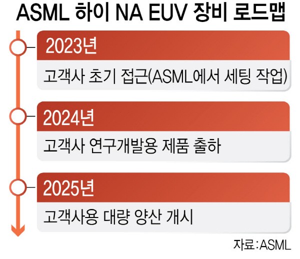
As all global semiconductor manufacturing companies place orders for ASML high NA EUV equipment, fierce competition is expected to unfold from 2025, when mass production begins. High NA EUV equipment is more expensive than currently used EUV equipment, but it can implement ultra-fine processes at once (single patterning), which can dramatically increase productivity. In the case of Samsung Electronics, it is necessary to preemptively secure highNA EUV equipment for 2-nano mass production after 3-nano mass production. Existing EUV equipment is estimated to cost 200 billion to 300 billion KRW, and high NA EUV equipment is estimated to reach 500 billion KRW.
ASML announced on the same day that it recorded net sales of 5.8 billion EUR, gross margin of 51.8%, and net profit of 1.7 billion EUR in the third quarter. Net sales for the fourth quarter are expected to be between 6.1 and 6.6 billion EUR.
Peter Wennink, CEO of ASML, said“Market uncertainty exists due to a number of global macroeconomic concerns, including inflation, consumer confidence index, and recession risks, however, overall demands for ASML system are very strong. As a result, in the third quarter, we recorded the largest quarterly reservation sales of about 8.9 billion EUR, including 3.8 billion EUR in EUV equipment sales such as high NA systems.”
By Staff Reporter Dong-jun Kwon (djkwon@etnews.com)