Providing 17 times in 12-inch, 12 times in 8-inch
Fabless and government accepting 'expansion request'
The first '4-nano advanced process' next year included
Fabless securing ‘prototype productio
Samsung Electronics' foundry will increase the number of 'multi-project wafers' (MPW) next year by 20% compared to this year. MPW is fabricating of different semiconductor fabless prototypes on wafers, which is necessary for the development of new chips. It is expected to help fabless to improve semiconductor performance through various product development and pre-production.
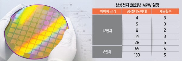
Samsung Electronics' foundry MPW will operate 29 times in total next year, 17 times in 12-inch and 12 times in 8-inch. It is 6 times more than this year's 23 times (13 times in 12-inch, 10 times in 8-inch). Although it is slight increase by about 20%, however, considering that several fabless can participate in one MPW process, the opportunity to make prototype semiconductor chips will be greatly expanded. The semiconductor fabless industry is highly encouraged.
Samsung Electronics reduced the number of this year’s MPW by about 43% compared to the previous year. In particular, the number of 8-inch MPW has been reduced by more than half. This was the reflected result of foundry bottleneck effect and demands. It is analyzed that the impact of the semiconductor supply shortage centered on 8-inch played a big role from the end of last year to the beginning of this year. The industry has continuously requested to expand the MPW line to support fabless. The 'Fabless-Foundry Coexistence Consultative Organization' launched by the Ministry of SMEs and Startups in January this year also selected the expansion of the small and medium fabless MPW process as a key task and started to come up with alternatives. As Samsung Electronics is the only one that can provide 12-inch foundry MPW in Korea, MPW expansion has rapidly emerged as a core concern of the industry.
The expansion of MPW is interpreted as a result of accommodating the requests of the fabless industry and the government. The road has been created for domestic fabless to develop semiconductor prototypes using Samsung Electronics' advanced foundry process. It is expected that the trouble of finding an overseas foundry to utilize the 12-inch MPW will be reduced. Next year, for the first time, Samsung Electronics' 4nm advanced process will be included in MPW. It seems that the stability of Samsung Electronics' 4nm process has been secured. It is expected to contribute to the development of advanced semiconductors such as mobile and high-performance computing (HPC).
◇Terminology
Multi-Project Wafer (MPW) = A service for manufacturing semiconductor prototypes for multiple customers with one wafer or for making multiple prototypes for a customer. The foundry provides this service to semiconductor fabless, universities, and research institutes that lack research and development (R&D) and prototype development capabilities. Although the foundry charges their customers, the government has recently been subsidizing some of the costs.
By Staff Reporter Dong-jun Kwon (djkwon@etnews.com)