Korea Fabless Industry Association is launching the 'Multi Project Chip (MPC)' project to promote coexisting relationship between semiconductor fabless and foundries to strengthen the national system semiconductor capabilities. It is a new concept pre-production method that implements specialized semiconductor design technology for each fabless in one chip. The association expected that MPC would not only reduce costs of system semiconductor development but also increase prototype production yield.
Korea Fabless Industry Association recently selected MPC as a key business and started a demand survey for Korean semiconductor fabless. They plan to establish a business cooperation system with government organizations that support the production of system semiconductor prototypes and foundries.
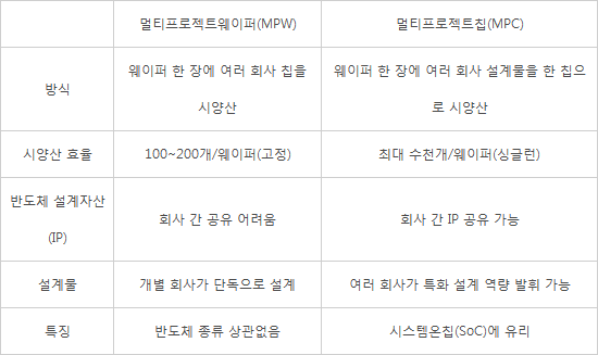
MPC was first proposed by the association as an improved concept of 'Multi-Project Wafer (MPW)', which makes semiconductor prototypes from several existing companies at foundries. Related patents are also pending.
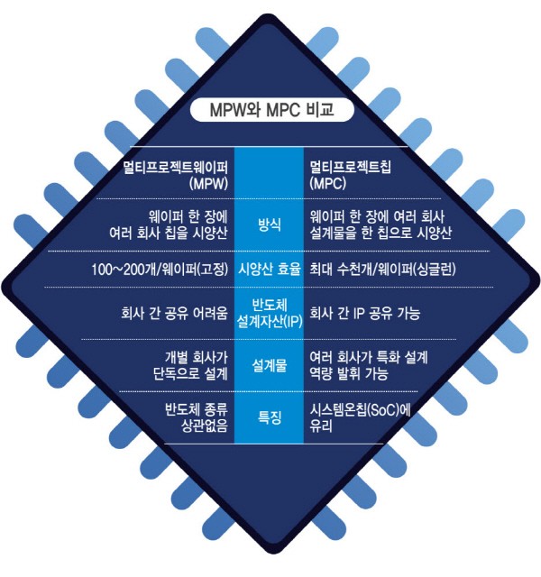
MPC is still the same as the existing MPW the fact that several companies participate in the mass production of semiconductors. MPW is a method that semiconductor chips from multiple companies are made on a single wafer. On the other hand, in MPC, semiconductor intellectual property (IP), cores, libraries, and software (SW) are implemented in one chip on one wafer. The representative system on a chip (SoC) structure is advantageous for developing high-performance and high-quality system semiconductors by combining different capabilities of each fabless company.
The association predicted that MPC would maximize the efficiency of commercial production. MPW allows that company to produce 100~200 chips per wafer. Since MPC allows many numbers of prototypes that can be made per wafer, semiconductor designs from multiple companies can be implemented on a single chip. With ‘single run’ standard, it is estimated that thousands of prototype products can be produced. If they can raise the efficiency of prototype, many customers can check the product and run reliability test before the mass-production.
MPC can also contribute to improving the poor IP utilization ecosystem. Fabless and foundries participating in MPC can reduce design and development costs in various ways, such as joint licensing to produce a single prototype chip. In addition, the relatively lack of IP can be greatly improved by mutual sharing between MPC companies.
The association judged that in order for the MPC project to be actively used, the participation of many companies and institutions is necessary. In order to achieve this, a full-scale MPC ecosystem will be created from this year. As the industry is unfamiliar with MPC, they plan to expand the number of participating companies through various activities such as spreading the concept.
Hyo-seung Lee, vice chairman of Korea Fabless Industry Association (CEO of NeoWine), said, “The association has prepared MPC as a way to improve the stagnant semiconductor competitiveness of Korea and take the national economy to the next level. It will be a 'win-win' strategy where fabless can reduce their development cost and secure high-quality semiconductor and foundry can efficiently operate the process.”
[Comparison between MPW and MPC]
By Staff Reporter Dong-jun Kwon (djkwon@etnews.com)