A-PRO Semicon will develop next-generation gallium nitride (GaN) power semiconductor foundry process technology with DB HiTek. GaN is considered a next-generation power semiconductor material.
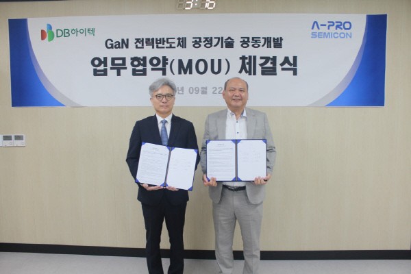
On the 22nd, A-PRO Semicon exchanged a memorandum of understanding (MOU) with DB HiTek for the development of GaN foundry (consignment production) process technology at the A-PRO headquarters in Gunpo-si, Gyeonggi-do. The process technology is 8-inch for the production of GaN power semiconductors. The US, Europe and Japan lead the GaN semiconductor market. Beginning with 4-inch process technology, the development of 6 and 8-inch GaN semiconductors is in process.
A-PRO Semicon is developing an 8-inch GaN semiconductor process with DB HiTek. The company will complete the development of the technology for GaN semiconductor mass production by 2024. The companies will cooperate in materials, parts, and equipment for the production of 8-inch power semiconductors that are larger than 4 and 6-inch semiconductors. It is expected that A-PRO Semicon will promote an epiwafer, which is a GaN base material, and A-PRO will cooperate with necessary materials.
An official from A-PRO said, "We are very pleased to have signed an agreement with an 8-inch foundry leading company in Korea. We will create a good opportunity to have a synergy effect in GaN power semiconductors based on our GaN technology.”
A-PRO Semicon's GaN process technology cooperation is due to securing next-generation power semiconductor manufacturing technology. It is anticipated that the company has secured a stable foundry production capability in the future by utilizing DB HiTek's 8-inch semiconductor process equipment compatibility. Even though A-PRO Semicon is a semiconductor fabless (design) company, it possesses GaN epiwafer manufacturing technology and GaN power semiconductor process technology. With DB HiTek and GaN power semiconductor process technology, A-PRO Semicon is expected to secure a stable production capability.
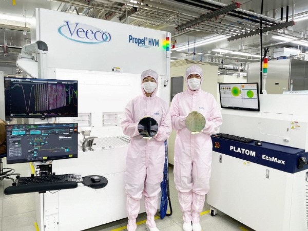
DB HiTek plans to purchase and utilize A-PRO Semicon’s epiwafers. GaN epiwafers are a key material that is being heavily dependent on foreign imports, and requires more advanced technology than existing wafers. A-PRO Semicon brought in an epiwafer manufacturing equipment, metalorganic chemical vapor deposition (MOCVD), to produce epiwafers from Korea. According to a market research firm, Yole Developpement, the GaN market is growing at an average annual rate of 49%, from this year’s $270 millio to $2 billion in 2027. An official from DB HiTek said, "We have secured a future growth driver in cooperation with A-PRO Semicon, and laid the foundation to lead the next-generation high value-added power semiconductor market that is rapidly growing." A-PRO and DB HiTek will have a synergy effect by building a power semiconductor supply chain and increase sales from localizing GaN power semiconductors.
By Staff Reporter Ji-woong Kim (jw0316@etnews.com)