Take on the challenge of miniaturizing and making processes eco-friendly
Technological difficulty has increased so it cannot be solved alone
Emphasis on cooperation between design, materials, parts, e
The creation of an unprecedented 'collaboration ecosystem' was ordered, in order to break through the limitations that semiconductor technology leaders currently face. It was pointed out that, without mutual cooperation between semiconductor design, materials, parts and equipment (MPE), and manufacturing companies, it is impossible to respond to the era of advanced processes represented by 3 nanometers or less.
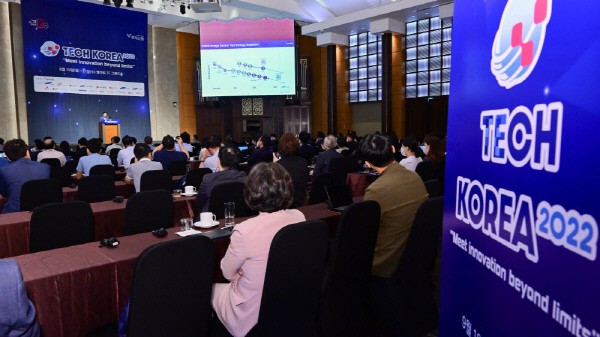
Speakers presented all-round collaboration as a method to overcome the challenges faced by the semiconductor industry, at the 'Tech Korea 2022' semiconductor session held at the EL Tower in Yangjae-dong, Seocho-gu, Seoul on the 19th, which was hosted by the ET News. Yoo-kyun Shin, vice president of Samsung Electronics, said “In order to overcome the challenges that the semiconductor industry faces and prepare for the future, innovation in the entire semiconductor ecosystem is essential,” and emphasized that, “Only when innovation in all-round technologies such as design and electronic design automation (EDA) technology is supported along with material, facility, process, and structural innovation can we overcome the constantly increasing technological barriers and move forward.”
Jong-hwan Kim, vice president of SK Hynix, also said, “In 10 years time, the difficulty of semiconductor technology will further increase and there will be challenges related to energy,” adding that, “Suppliers, academia, and the government must work together to respond to the future environment.”
This means, 'the semiconductor industry must immediately take on the challenge of overcoming the limitations of process miniaturization and implementing eco-friendly technologies, and in the manufacturing field, it is necessary to prepare for the era of advanced processes of 3 nanometers or less, and there also needs to be technologies that maximize power efficiency, as well as a responsive strategy.' There are many concerns that semiconductors cannot process data, which is expected to reach 175 zettabytes (about 175 trillion gigabytes) by 2025, if these challenges are not addressed.
As technological difficulties increase, it is becoming increasingly impossible for a specific company to solve these problems on its own. This is the basis for the increasing number of cases for partnerships between material parts and equipment companies to discover new materials, develop new materials, and process equipment to use them.
A prime example is cooperation between semiconductor materials, parts, equipment, and manufacturing companies. Applied Materials is focusing their attention on new materials, as a key technology to realize semiconductor innovation. It is strengthening the cooperative system throughout the material supply ecosystem so that new materials can be applied to the development of semiconductor process equipment. The goal is to improve semiconductor power, performance, area, cost, and time to market (PPACt).
Lam Research also operated a Korean R&D center to realize the performance and technology required by semiconductor manufacturers such as Samsung Electronics and SK Hynix. As for semiconductor equipment, ties between manufacturing and material and parts suppliers in Korea will further be expanded. ASML also opened the door to cooperative R&D with materials, parts and equipment companies and semiconductor manufacturing companies to develop next-generation extreme ultraviolet (EUV) exposure equipment.
The general consensus within the industry is that semiconductor investment should also be focused on creating a robust ecosystem. Hong-Joo Baek, CEO of Wonik QnC, said, “Long-term physical and human investment is required in order develop technology throughout the semiconductor ecosystem,” furthermore, “In particular, it is necessary to nurture manpower and create a pool through industry-university-institute collaboration” CEO Baek added, “We also need active technology exchanges between individuals that are experienced in semiconductor processes and material development personnel.”
By staff reporter Dong-joon Kwon djkwon@etnews.com