The world’s largest NAND flash manufacturing facility
Production facility for EUV process-based DRAM is also planned
Construction of ‘P4’ in preparation in response to demand in semiconductors
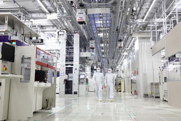
Samsung Electronics has started its operation of the world’s largest semiconductor manufacturing facility ‘P3’ in Pyeongtaek. Since July, Samsung has established a mass-production facility for NAND flash and started wafer insert. It has been about two years since the initial construction in 2020.
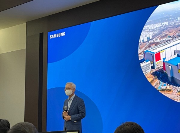
Kye-hyun Kyung, CEO, and president of Samsung’s device solutions division, met with reporters and presented a growth strategy based on “Focusing on Samsung’s strengths.”.Regarding Samsung Electronics Vice Chairman Jae-yong Lee’s announcement ‘Global No.1 in System Semiconductors by 2030” in 2019, CEO Kyung quoted, “We are analyzing on how we can become the first place.”.
CEO Kyung also added, “Customers are interested in the second generation of 3-nano Gate-All-Around to be mass-produced next year. If we actively develop the 3-nano process and focus on improving the performance of the 4th and 5th generation processes (Which were relatively behind), the outlook of Samsung Electronics’ foundry will be more positive.” As he showed high expectations in the world’s first mass production of 3-nano process technology which succeeded in June. Regarding the application processor (AP) Exynos, which has suffered a performance controversy, he explained, "We are focusing on what we can do best with our current development capabilities and how to restore competitiveness."
Samsung Electronics is expanding its market dominance through the mass-production of NAND flash in P3. With the single line alone being 700m, P3 is the world’s largest semiconductor manufacturing facility. The total area is 991,000 square meters, which is equivalent to the size of 25 soccer fields. P3 is also the location where President Suk-yeol Yoon and U.S. President Joe Biden visited to pledge a “Semiconductor Alliance.”
To meet market demand, Samsung Electronics is planning to establish high-tech process production facilities such as extreme ultraviolet (EUV) process-based DRAM and foundries for 5-nano or less. Preparations for the construction of the fourth plant (P4) within Pyeongtaek Campus has also begun. Although the time of construction and products to be produced remains undecided, it is in preparation to quickly respond to changes in demand for semiconductors.
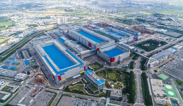
The Pyeongtaek Campus, which Samsung Electronics has been constructing since 2015, has a total area of 2.89 million㎡. This is equivalent to both areas of Giheung Campus (1.45 million㎡) and Hwaseong Campus (1.58 million㎡) combined.
Samsung Electronics held a groundbreaking ceremony for the GIheung R&D Complex last month. While accepting the prospect of the outlook of the semiconductor industry being bleak until next year, he said, “We will consistently proceed with the direction of our fundamental investmentregardless of the situation of the current market.” Regarding external environmental risks such as the U.S. restrictions on exports of semiconductor equipment to China, he added, “It is true that the amount being supplied to China is large and that it is an important market, but we are seeking for a method to be beneficial to all parties within a difficult situation.”
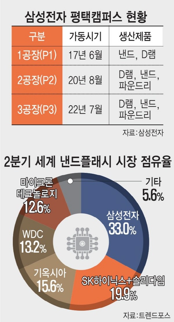
According to the market research firm TrendForce, Samsung Electronics recorded 5.98 billion USD (About 8.2494 trillion KRW) in NAND flash sales in the second quarter. It ranked first place globally with the market share of 33%. Samsung Electronics kept its place in the lead since it topped the NAND flash market in 2002.
By Staff Reporter Yoon-sub Song (sys@etnews.com)