Synopsys to provide EDA solution in the form of SaaS
Subscription-based service... Investment cost savings effect
License management expected to be more convenient
The movement to provide semiconductor circuit design software (SW) in a cloud environment has accelerated. Since the existing semiconductor consignment production (foundry), as well as the electronic design automation (EDA) tool industry, enters the cloud market, a major transformation is taking place in the 'software as a service (SaaS)' based semiconductor design environment.
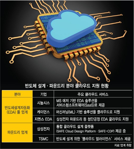
Synopsys, the world's largest EDA company, has recently begun supplying EDA solutions in SaaS form. Although rivals Cadence and Siemens EDA supported major semiconductor design software functions in the cloud, Synopsys is the first to provide the entire solution in the form of SaaS. SaaS refers to a software supply method in which a solution is subscribed according to the usage period and capacity, rather than as a single package.
Synopsys will provide semiconductor design software via 'Azure', a cloud service by Microsoft (MS). Fabless companies that design semiconductors can pay prices according to their usage of the cloud service provided by Synopsys. It's a pay-as-you-go system. It may be operated as subscription-based rather than the existing single package purchase method.
Semiconductor fabless companies do not need to build large-scale computing infrastructure to design semiconductors. They can access advanced semiconductor design environments provided by Synopsys through the cloud service. It could also be an opportunity to reduce investment costs for semiconductor design. Synopsys is advantageous in that it can thoroughly manage EDA solution licenses. The EDA tool license cost is considered to be one of the main factors causing price negotiations between suppliers and fabless.
As Synopsys actively enters the cloud market, the EDA tool market is expected to change. This is because the existing cloud-based semiconductor design support service was limited to the foundry industry. Samsung Electronics has provided the 'Integrated Cloud Design Platform (SAFE-CDP)' since 2020, for semiconductor design convenience for its foundry customers. It is supporting domestic fabless companies to enter the semiconductor design market without large-scale information technology (IT) infrastructure, such as private servers. TSMC is also operating a service that provides semiconductor design in a cloud environment through the 'Cloud Alliance'.
In the future, major EDA tool makers are expected to accelerate their transition to cloud. EDA tool license management has become difficult as the number of semiconductor design personnel used in advanced processes under 7nm has increased. Converting this to a cloud subscription model can increase the convenience of license management. A semiconductor fabless official said, "The cloud can be advantageous in reducing the costs of establishing a semiconductor design computing environment suitable for high-tech processes," but added, "However, there are concern that there will be less room for price negotiations since license costs are fixed."
By Staff Reporter Dong-jun Kwon djkwon@etnews.com