A domestic company is standing out in the printed circuit board (PCB) inspection equipment market, which Japan had a monopoly over. The adoption rate of domestic equipment has increased after the trade dispute between South Korea and Japan, and the market share of the domestic equipment industry is expanding as the semiconductor substrate industry enters a boom.
According to the parts and equipment industry on the 11th, the semiconductor measurement and inspection equipment market has grown to KRW 1 trillion annually. Even 10 years ago, all Japanese equipment had to be imported, but the market share of domestic equipment is growing rapidly.
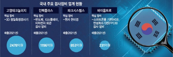
Founded in 2000, Bioptro is developing flip-chip ball grid array (FC-BGA) equipment, following inspection equipment for high-density interconnect (HDI) boards and flexible printed circuit boards (FPCB). It plans to strengthen its new business by launching new inspection equipment for FC-BGA boards this year.
The FC-BGA inspection equipment market is technically difficult, and Japanese companies have had a monopoly over it until now. Since demand for FC-BGAs in Japan also increased, equipment makers such as Nidec Corporation focused on responding to the domestic market. Due to the trickle-down effect, Bioptro is expected to increase its market share by localizing FC-BGA inspection equipment this year.
Intekplus, a company specializing in semiconductor, display, and secondary battery exterior inspection equipment, is expected to record their highest sales this year as the adoption rate of inspection equipment by Outsourced Semiconductor Assembly and Test (OSAT) companies is increasing. Intekplus, which has machine vision technology, has 2D and 3D automatic exterior inspection equipment that analyzes and processes image data on representative features.
The semiconductor inspection equipment, which Koh Young Technology is promoting as a new business, is also expected to enter a full-fledged growth trajectory this year. Meister D+, developed by Koh Young Technology, is the world's first inspection equipment that simultaneously measures the exterior and surface of manual semiconductor parts in the semiconductor post-processing. Recently, the demand for back-end process equipment has increased as electronic circuits have become highly integrated.
Park Systems, which develops Atomic Force Microscopy (AFM) Systems, is expanding its business to industrial use from their current academic research market. This is due to the increased demand for inspection through atomic force microscopy as semiconductor substrate refinement processes have expanded.
Park Systems garnered attention for precise measurements with its technology to separate products or samples without damages. It is expanding its business field to various fields such as display panel processes as well as semiconductor processes.
An official from the parts industry said, "Although the market share of Japanese equipment industry such as Omron and Advantest is still high, the competitiveness of domestic companies have recently been attracting attention for after-sales service (AS) and technical response," adding, "As demand for semiconductor substrates have recently increased, the domestic inspection equipment industry is also expected to perform well."
By Staff Reporter So-ra Park srpark@etnews.com