Possibility of single chip integration of CPU·memory
Advance implementation of a computer smaller than a phone
Unlimited usage in IoT and AI fields
A research team at Hanyang University has developed a new semiconductor element technology that can implement microcomputers.
Hanyang University announced on the 18th that a team led by Professor Jae-kyung Jeong of Convergence in Electronics in the College of Engineering has developed a world-class 'p-channel transistor' element with application of Tellurene 2D semiconductor material.
It is a technology that makes it possible to implement CMOS TFT peripheral circuits required for memory (RAM) device integration in three dimensions on top of an existing silicon processor (CPU) in order to create a single integrated chip with CPU and RAM combined.
A single chip cannot be manufactured with existing technology. When the technology is commercialized, the area occupied by the CPU and RAM will be reduced, making it possible to manufacture ultra-small computers and make smartphones smaller.
In addition, the physical wiring distance between the CPU and RAM is shortened and the vertical wiring density is dramatically increased, so that calculation and processing speed are more than doubled, and data can be exchanged 10 times or more.
Professor Jeong participated in organic light emitting diode (OLED) R&D at Samsung Display before working at the school.
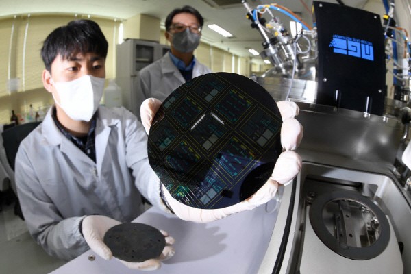
The research team has developed a high-quality two-dimensional Tellurene thin film manufacturing method using sputtering and ALD processes that can be easily applied in the semiconductor and display industries beyond academic research.
Currently, memory and logic semiconductor elements integration improvement has faced a physical limit, as the individual transistor size reaches the nano level. As a result, two-dimensional Tellurene semiconductor materials are attracting attention among global research.
In order to apply a two-dimensional semiconductor material to a semiconductor process, it is necessary to develop a technology that can grow it on a 12-inch wafer at a temperature of 400 degrees or less. However, the solution-based or cryogenic deposition reported so far has a problem in that it is difficult to apply to the existing semiconductor process.
Professor Jeong's team presented a growth method that can uniformly form a two-dimensional Tellurene thin film even at room temperature on a 4-inch wafer substrate through the 'physical vapor deposition method', which is easy to apply to existing semiconductor processes.
At the wafer level, the p-channel FET device to which the two-dimensional Tellurene channel is applied showed excellent performance, such as a field mobility of 30㎝2/Vs or more and a current flash ratio of 105 or more, even at a gate voltage as low as 5V.
This is the world's best performance based on the characteristics of the deposition-based p-channel FET element reported so far. Since the maximum temperature of the manufacturing process is about 200 degrees, it is possible to vertically integrate three-dimensionally on a silicon CPU. It is meaningful in that it can be used not only in the 'monolithic 3D integrated device' that implements a processor and memory in a single semiconductor chip in the future, but also in the field of mobile displays that can be used for several days on a single charge.
Professor Jeong said, “The high-performance p-channel 2D tellurium-based transistor process technology can be directly applied to the upper layer of monolithic 3D integration technology in the future. Not only be able to create single system semiconductor combing memory·logic, it will be possible to use it in various fields such as the Internet of Things (IoT) and artificial intelligence (AI) in the future that requires multifunction and extreme low power.”
The research was conducted with support from the National Research Foundation of Korea research support program and LG Display. The research results were published in a world-renowned academic journal in the field of materials (npj 2D Materials and Applications).
It was conducted in a joint research format with Seung-wu Han from Seoul National University, Seong-yoon Jeong from KAIST, and Professor Kwon-beom Jeong from Dongguk University, and researcher Tae-gyu Kim (in process of doctoral program) participated as the first author from Hanyang University, Department of Electronic Engineering, Convergence in Electronics.
By Staff Reporter Myung-hee Kim (noprint@etnews.com)