Intel is launching an all-round strategy to seize the semiconductor hegemony. From semiconductor structure (architecture) to process technology and manufacturing, Intel has transformed all the core competencies of a semiconductor company. It is understood that Intel is taking an opportunity where the global supply chain is shaken due to a shortage of semiconductors, and is actively strategizing to regain the title of 'Intel of technology’. These are changes came within a year since Intel CEO Pat Gelsinger took office.
Intel is on the spotlight for how its internal and external changes will affect the global semiconductor market. After Intel unveiled semiconductor architecture and new process technology, it is noteworthy whether the semiconductor competition will change as Intel expands its business area with unprecedented aggressive investment.

At the 'Oregon Business Plan Leadership Summit' held earlier this month in Oregon, U.S., CEO Gelsinger once again emphasized the importance of semiconductor manufacturing and supply chain. He predicted and said, "Tens of thousands of dollars worth of cars cannot completed due to a two-dollar chip. Semiconductor currently accounts for 4-5% of auto parts, but by 2030, it will account for 20% of electric vehicle parts.
Market demand increased sharply due to a shortage of semiconductor supply, and CEO Gelsinger predicted that this situation will be prolonged. This is due to the dependence of all kinds of products on semiconductors is increasing. The current situation is an opportunity for Intel. This is why CEO Gelsinger is showing interest to the semiconductor architecture, process, and manufacturing roadmap.
◇Resumed developer forum after 10 years... Next-generation architecture revealed
Last October, Intel held an 'Intel Innovation' event. It is the first time in 10 years since Intel opened a developer forum to discuss development of a developer-centered innovation model and community support. CEO Gelsinger is one of the founders of the early Intel developer forum. The role of CEO Gelsinger was critical the resurgence of developer-centricity. He said, “Developers are true superheroes in the digital world based on semiconductors. Intel will utilize every element to unlock the infinite possibilities of silicon (semiconductor).”
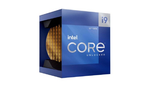
Developers are at the heart of Intel's technological innovation. CEO Gelsinger wanted to further advance Intel's technology through developer support. His intention was clearly revealed at Intel Architecture Day. In September, Intel launched an 'Efficient' core that will run low-power mobile applications, and introduced the first hybrid architecture Intel 'Alder Lake' equipped with a 'Performance' core that acts as a high-performance brain. Thread Direct, Intel's proprietary technology for seamless interworking between Efficient and Performance Core, was also introduced for the first time. This innovative technology announced the return of the powerful 'Intel 12th generation core (code name Alder Lake' and central processing unit for PC) released in November. It showed a significant performance improvement compared to the previous generation. It elicited the evaluation of 'Intel is Back' from various reviewers.
Intel is also planning to release a server CPU, codenamed 'Sapphire Rapids’, in the first half of next year. Expectations are high that it will induce new server demand and drive the boom in the memory market.
◇The end of the nano era... The era of Intel's 'Angstrom' opens.
Among the 'surprise announcements' of Gelsinger this year, Angstrom stood out. Until now, semiconductor processing technology has been represented by nanometers. However, as process miniaturization accelerated, it became increasingly difficult to represent advanced process technology with nanometers. However, Intel is competing with Angstroms, which means 0.1 nanometers. It is also a card that Intel used as a strategy to differentiate itself from competitors when it announced its re-entry into the foundry market earlier this year.
Intel will introduce advanced process technology equivalent to the industry's 2nano process in 2024 under the new name of 20A. Until then, Intel presented Intel 7, Intel 4, and Intel 3 ultra-fine process roadmaps. Intel dismissed industry concerns about the slow transition to advanced processes from 10nm.
Some pointed out that the future is rosy. However, Intel secured customers based on trust in technology. Qualcomm plans to mass-produce chips from 2024 using the ultra-fine process of Intel's foundry. Intel has decided to launch 18 Angstroms by 2025.
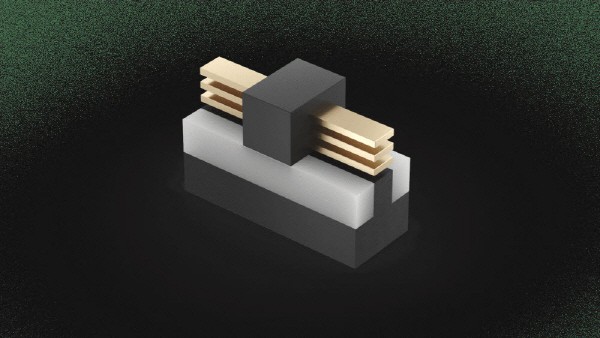
This strategic roadmap is due to the Intel transistor structure that has changed in 10 years. The FinFET process, which has led the semiconductor industry for the past 10 years, was also applied by Intel for the first time. In the era of the angstrom process, Intel applies the ‘RibbonFET' of the gate all-around (GAA) method, which is a next-generation semiconductor transistor structure. It also unveiled 'Powervia', the industry's first semiconductor rear power supply technology, to secure leadership in advanced semiconductor process technology.
Along with EMIB, the next-generation packaging technology, Intel also set a packaging roadmap going from 'Foveros → Foveros Omni → Foveros Direct’. Amazon Web Services (AWS) is the first customer of Intel's advanced packaging solution.
◇ Large-scale investment in foundry and packaging makes 'Intel of Technology' a reality
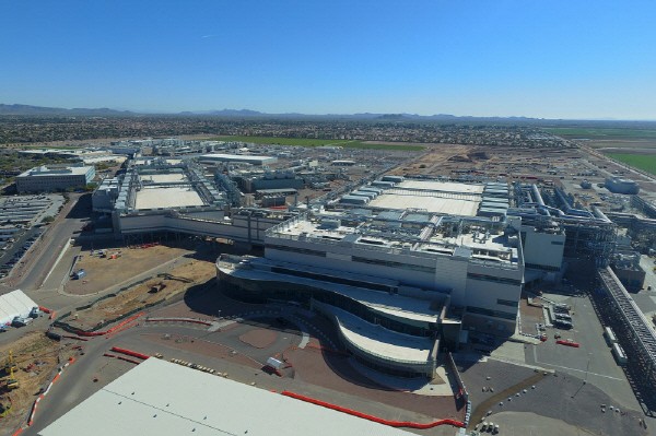
In order for the integrated device manufacturer vision (IDM 2.0) blueprint proposed by CEO Gelsinger to become a reality, a large-scale investment must be preceded. After taking office, he decided to pour $20 billion into the establishment of a U.S. semiconductor factory (fab) and started investing in earnest. It is investing not only in the U.S. but also in Europe to develop its foundry capabilities.
Packaging investment, another wing of Intel's semiconductor resurgence, is also assertive. Intel announced an investment of $3.5 billion to build a semiconductor back-end process facility in New Mexico in May. Intel is taking a multi-faceted approach to find new investment candidates. CEO Gelsinger is personally visiting overseas to discuss and support investment in semiconductor manufacturing bases with leaders from each country.
Due to the characteristics of the semiconductor market, Intel's investment is expected to achieve tangible results in two to three years. There is a long way to go until the moment when Gelsinger CEO's IDM 2.0 bears the fruit, but it is predicted that the market ripple effect will be formidable. The industry's attention is focused on Intel's move to regain the technology throne.
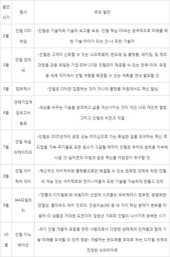
<Key remarks by Intel CEO Pat Gelsinger>
By Staff Reporter Dong-jun Kwon (djkwon@etnews.com)