Produced various standard and size packages at the same time
Commercialized 'Multi Array Substrate'
Targeted small and medium-sized fabless and university R&D markets
Preparing to apply for patents
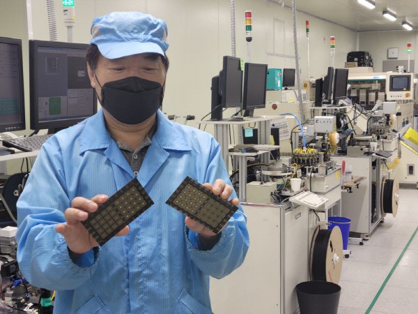
SNPT, a small and medium-sized semiconductor packaging company in Korea, has commercialized a technology for packaging semiconductors of various standards at once. By overcomingthe existing method’s limitations of packaging only one semiconductor per substrate, it can dramatically shorten the production period of semiconductor chips (samples) for development.
SNPT has started full-fledged commercialization by providing new packaging technologies to Korean semiconductor manufacturers and fabless. According to industry on August8, SNPT commercialized the 'multi-array structure semiconductor substrate' technology that simultaneously manufactures semiconductor packages of various standards and sizes.
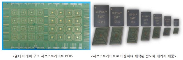
The company completed the patent registration in June and applied the technology to development semiconductor packaging process to domestic semiconductor manufacturers and six fabless firms. SNPT is the first to package development semiconductors of multiple standards in one substrate. In the semiconductor packaging process, a substrate is an auxiliary plate inserted between a printed circuit board (PCB) and a semiconductor and is used to electrically connect the semiconductor (die) cut from the wafer to the outside.
Although substrate-free packaging technology has emerged with the recent emergence of advanced packaging technologies such as wafer level packaging (WLP),it is still positioned as a dominant technology in the market. It is known that 80% of the total packaging market applies substrate. In the past, only one semiconductor could be packaged with one substrate. For example, two substrates are required to develop a 'four-way surface mount packaging' (QFP) compliant chip having semiconductor legs (lead pins) in all directions and a 'Ball Grid Array' (BGA) compliant chip with balls placed on the bottom of the package, instead of lead pins. However, this method consumes many substrates and takes a long period for package manufacturing, which can delay the development of new semiconductor products.
Hee-yong Yoon, head of S&PT Research Center (Vice President), said, “Semiconductor packaging for development involves many small batches of various types, so it took about 4 to 8 weeks to produce samples when using multiple substrates. We have to import most of semiconductor substrates for development because they are highly dependent on overseas.” The method developed by SNPT can respond to more than 10 semiconductor packaging standards with one substrate. It can also package different sizes of semiconductor by cutting the substrate differently, even with the same standard.
This can significantly shorten the development period for fabless chips that are produced in multiple samples, because several types of semiconductors can be manufactured at the same time. SNPT has explained that a small number around 100 of semiconductor chips for development is supplied, so samples can be supplied within 1-2 days at the earliestafter packaging.
SNPT plans to actively target the semiconductor market for R&D, such as small and mid-sized fabless and universities that design and develop semiconductors. It is also preparing to apply for overseas patents in the US and China. CEO Tae-nam Jeon of SNPT, said “Our technology will be able to shorten the manufacturing period for development semiconductors and save cost, which will contribute to strengthening the competitiveness of domestic fabless companies. We plan to provide services to prevent any disruption to the new product development schedule due to packaging delays.”
By Staff Reporter Dong-jun Kwon djkwon@etnews.com