Appled Materials has introduced a semiconductor inspection system that is able to capture defects more accurately through AI technology. Its latest inspection system is expected to help semiconductor companies improve their yields and productivity.
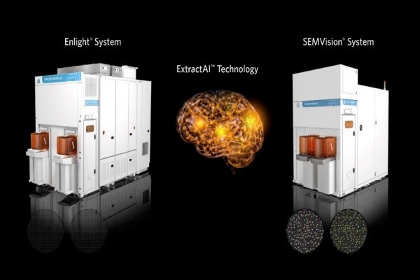
Applied Materials Korea held a press conference on Tuesday and introduced the company’s new semiconductor inspection system. At the conference, it introduced ‘Enlight’ wafer inspection system, SEMVision review system, and ExtractAI technology.
What is special about the systems that the company introduced at the conference is that they utilize AI technology. ‘Enlight’ inspection system captures any foreign substance or defect that is created during the wafer manufacturing sequence and moves data to an electronic beam equipment called ‘SEMVision’ system and utilizes AI technology to analyze possible causes that lower yields. The ExtractAI technology is the one that connects big data from the Enlight system to the SEMVision system.
Applied Materials Korea said that the company’s latest inspection systems and technology sort characteristics of wafer signals based on big data and analyze causes that may lower yields.
The Enlight inspection system in particular took about five years just for its development period. The system is able to perform more accurate inspection as it performs brightfield inspection technique and ‘greyfield’ technology at the same time.
Applied Materials Korea explained that increased complexity of semiconductor design and process led to the development of the two inspection systems. More accurate inspection systems are now needed by semiconductor companies as level of integration of chips becomes higher due to 3D-based devices and number of steps has increased by 45% compared to the past.
The company said that its inspection systems will help semiconductor companies save their costs at least by three times. With improved production costs, they can install even more inspection systems at their production lines and drastically increase yields from each process.
It also added that Applied Materials is currently supplying the two systems and the technology to a cutting-edge foundry company that manufactures system semiconductors.
Lee Seok-woo, who is an executive director at Applied Materials Korea, said that the two inspection systems’ ability to separate defects automatically has received positive feedbacks from customers and that he expects the two systems will be supplied for memory lines as well in the future.
Staff Reporter Kang, Hyeryung | kang@etnews.com