Samsung Electronics announced that it would be the leader in global markets for next-generation NAND flash memory and DRAM through different technologies.
The company held “Investor Forum 2020” for its investors on Monday and explained about its next-generation memory technologies.
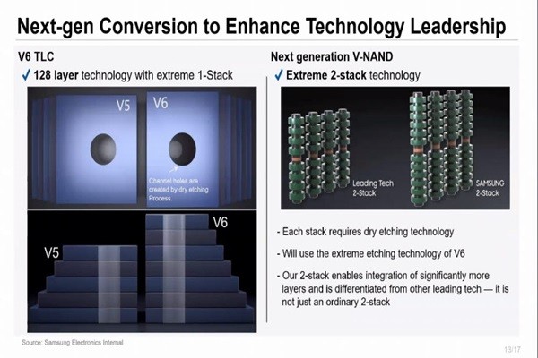
Han Jin-man, who is an executive director at Samsung Electronics, made an announcement during his presentation about Samsung Electronics’ strategy against COVID-19 and prediction on future memory market that the company’s 7th-gen NAND flash memories will be manufactured through “double-stack” technology.
Double-stack technology indicates a process that creates “channel holes”, which assist electric connection between layers in a stacked storage space at two separate times. Samsung Electronics has been using single-stack technology.
“We plan to introduce the advanced single-stack technology that we have been using for the 6th-gen NAND flash memories to the 7th-gen NAND flash memories.” said Executive Director Han. “We plan to implement a process that maximizes productivity.”
While stating that double-stack technology will increase unit cost by at least 10% due to an increase in number of processes, he emphasized that the company’s double-stack technology will not be anything like ordinary double-stack technology. He also added that the company has competitive edge in NAND flash memory technology over its competitors due to NAND flash memory height that is lower than its competitors’ products.
Because NAND flash memory is a chip that has storage spaces stacked vertically like an apartment, it is very important to lower a chip’s height while increasing number of stacked cells.
“Compared to our 92-layer TLC (Triple Level Cell) NAND flash memories, heights of 96-layer TLC NAND flash memories of our three main competitors are 30% higher at the most.” said Han. “We plan to realize different cost competitiveness with our advanced cell design and stacking technology.”
He also stated that the company would actively utilize EUV (Extreme Ultraviolet) technology in next-generation DRAMs and continue to lead the global DRAM market.
In 2020, Samsung Electronics became the first company to apply EUV process to 10nm-class (1z) DRAMs and it has been working on improving production yield of EUV-based DRAMs. Executive Director Han said that the company has established an inner EUV ecosystem and it has been managing an EUV task force.
Samsung Electronics predicts that the global DRAM and NAND flash memory markets will see higher growth in 2021. It estimated that bit growth for DRAM will increase by anywhere between high-teens to 20% in 2021 and that bit growth for NAND flash memory will increase by 30%.
The industry believes that Samsung Electronics will be very aggressive in making investments in memory facilities and equipment in 2021. Some predict that the company will make an investment that will lead to monthly production of 100,000 12-inch wafers that is equivalent to single semiconductor fab in the first half next year.
Meanwhile, key executives from Samsung Electronics’ semiconductor business such as Vice President Park Yong-in of System LSI Division and Executive Director Han Seung-hoon of Samsung Foundry in addition to Executive Director Han also had presentations on image sensor and Samsung Electronics’ foundry business at the forum.
Staff Reporter Kang, Hyeryung | kang@etnews.com