Samsung Electronics is set to invest $8.1 billion (10 trillion KRW) into Pyeongtaek Campus and construct its second “extreme ultraviolet (EUV)” foundry line in Pyeongtaek Campus after constructing its first EUV line in Hwaseong Campus. Its strategy is to prepare for growing demands for cutting-edge system semiconductor and to accelerate the process of becoming world’s best system semiconductor company by 2030. Regarding this investment, Vice-Chairman Lee Jae-yong of Samsung Electronics emphasized that future investments must be carried out even more during difficult times.
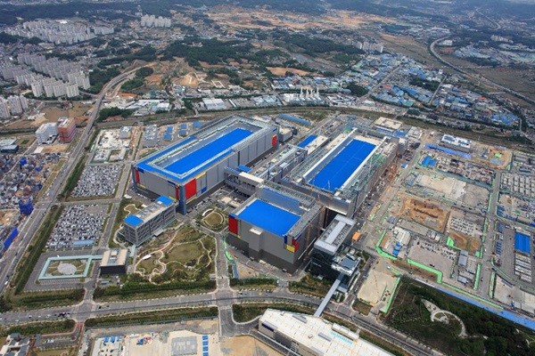
Samsung Electronics on May 21 announced that its Pyeongtaek Campus will be furnished with an EUV foundry line just like the Hwaseong Campus. Necessary equipment will be set up within the “P2” fab.
According to the industry, Samsung Electronics will invest about $8.1 billion to construct the new EUV foundry line. It is estimated that the size of initial production will be 15,000 chips per month. The new EUV foundry line will go through construction starting from this month and is expected to be in operation in the second half of 2021.
Foundry business refers to a business that manufactures chips for semiconductor design companies after receiving requests from them. Samsung Electronics currently has foundry lines in Hwaseong and Giheung and Austin, Texas.
The global system semiconductor industry prefers foundry processes that can manufacture chips that are miniature and applied with advanced functions due to the expansion of new markets such as 5G network and HPC (High-Performance Computing).
Samsung Electronics has actively working on growing its foundry business based on its vision of becoming the world’s best system semiconductor company by 2030 that it announced April of 2019. It has been also responding quickly to microfabrication demands from semiconductor design companies.
The EUV process, which is a nanofabrication process, is a prime example. Samsung Electronics was the first within the global foundry industry to utilize the EUV process, which utilizes a wavelength that is 14 times smaller than that of the ArF process, and has been manufacturing chips that are smaller than 7 nanometers.
After succeeding in manufacturing chips from the S3 line, which is located in the Hwaseong Campus, through the EUV process last year, it started operating the V1 line, which is designed specifically for the EUV process, on full-scale this past February and started manufacturing 7nm chips.
Many predicted that the Pyeongtaek Campus, which is furnished with the P1, P2, and P-EUV lines, will be the core manufacturing base for memory semiconductor. However, it is heard that Samsung Electronics decided to construct a new EUV foundry line within the P2 fab, which has plenty of unused space, as the space within the V1 fab has been filled to its maximum capacity. Samsung Electronics made plant and equipment investment in the P2 fab in order to manufacture 30,000 DRAMs monthly.
“We have expanded our nanofabrication production through the V1 line.” said a representative for Samsung Electronics. “Once the new EUV line goes into full operation, we will be able to manufacture chips based on nanofabrication at a much faster rate.”
Samsung Electronics is planning to manufacture chips smaller than 5 nanometers from the new EUV foundry line in Pyeongtaek. After manufacturing 5nm chips based on the EUV process first from the EUV foundry line in Hwaseong in the second half of this year, it is also going to manufacture 5nm chips as main products from the foundry line in Pyeongtaek.
“By increasing the production of chips smaller than 5 nanometers, we are going to actively respond to growing demands for cutting-edge semiconductors.” said President Jung Eun-seung of Samsung Electronics who is the head of the foundry business. “Through strategic investments and continuous hiring of talented individuals, we are going to continue solid growth of our foundry business.”
Staff Reporter Kang, Hyeryung | kang@etnews.com & Staff Reporter Yun, Geonil | benyun@etnews.com