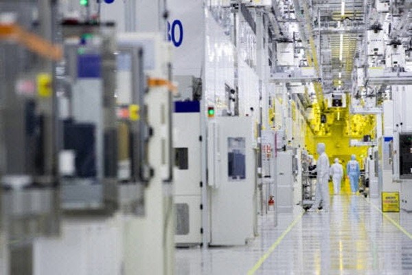
Samsung Electronics is applying its “super-gap” strategy to its NAND flash memory technology. It is understood that Samsung Electronics is developing 7th generation V-NAND flash memory with 160 layer or higher.
The number of layers is the most within the industry. There will be more uses to NAND flash memory, which stores data, as the number of layers increases which then leads to greater capacity.
Although a Chinese semiconductor company called YMTC recently announced its plan to mass-produce 128-layer NAND flash memory by the end of this year, Samsung Electronics is already preparing for the next generation.
According to the industry, it is understood that Samsung Electronics is developing 7th generation V-NAND flash memory with 160 layer or higher. It is heard that Samsung Electronics has already made a significant process as it has accelerated the development process.
Samsung Electronics is looking into applying “double-stack” technology to the 7th generation V-NAND flash memory. This technology creates holes in two separate times so that current can go through circuits.
Samsung Electronics has been using “single-stack” technology that creates holes all at once. It seems that Samsung Electronics is considering the “double-stack” technology due to an increase in the number of layers.
160-layer or higher NAND flash memory will be the first within the industry. The highest number of layers of currently commercialized NAND flash memories is 128.
No company has yet to announce that it has succeeded in developing 160-layer or higher NAND flash memory. Samsung Electronics and SK Hynix announced last year that they developed 128-layer NAND flash memory. YMTC recently succeeded in developing 128-layer memory as well and announced its plan to start mass-producing the memory by the end of this year.

Development of 160-layer or higher nand flash is expected to be an important stepping stone for Samsung Electronics to widen the technology gap between itself and its competitors.
In order to increase storage capacity, number of NAND cells (data storage space) needs to be increased.
“Stacking” technology was developed in order to increase number of NAND cells and it stacks NANDs that are flat vertically like an apartment in order to increase storage capacity.
The industry calls it 3D NAND flash memory while Samsung Electronics uses a name “V-NAND”. Number of layers indicates how many layers can be stacked and it is the key competitive edge of NAND flash. Samsung Electronics is seen as the company that is most advanced when it comes to this technology.
Samsung has also put efforts into the development. Vice-Chairman Kim Ki-nam of Samsung Electronics announced during a general meeting of shareholders that was held last month that the company would push for the development of “7th generation V-NAND” in order to separate the company from its competitors. This 7th generation V-NAND indicates 160-layer or higher NAND flash memory.
Samsung Electronics made $16.517 billion from the global NAND flash market last year which was the highest sales within the industry (35.9%). Despite the current situation on COVID-19, Samsung Electronics has been making investments continuously without any stoppage or reduction in order to achieve “super-gap” in both technology and production capacity.
Because SK Hynix has also resumed its investments in memory recently, it is expected that “super-gap” within the semiconductor industry, which is a pillar for the South Korean economy, will continue to take place for a while.
Staff Reporter Kang, Hyeryung | kang@etnews.com & Staff Reporter Yun, Geonil | benyun@etnews.com