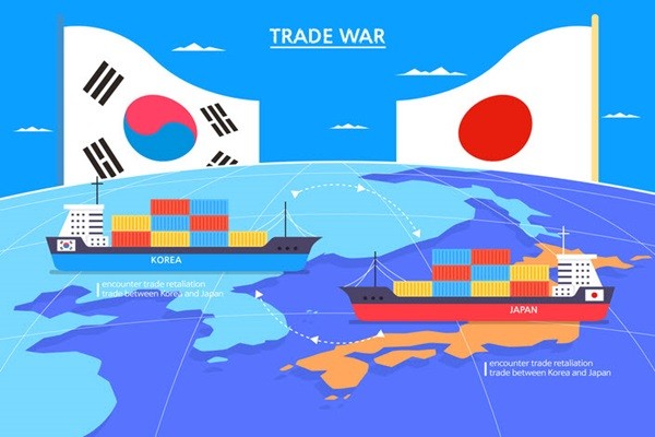
Japanese semiconductor materials makers are setting up their production bases in South Korea one after the other as they fear that they may be separated from global SCM (Supply Chain Management) as the Japanese Government’s trade restrictions on South Korea is dragging out. They are working on producing their products within South Korea by building research facilities and production bases of their major products in South Korea.
A chemical product maker called ADEKA is currently producing its strategic products from its production base in Jeonju. It is currently producing some of semiconductor materials that had been produced from its plant in Kashima from its base in Jeonju. The industry believes that ADEKA will produce “Cphafnium” for Samsung Electronics. Cphafnium is a precursor that is used to cover High-K dielectric film that blocks leakage current. Semiconductor device makers that have been using Cpzirconium are starting to use Cphafnium more due to microfabrication of DRAM. It is heard that ADEKA supplies significant amount of supply of high dielectric precursor for DRAM used by Samsung Electronics.
Kanto Denka Kogyo, which supplies NF3 to South Korean semiconductor manufacturers, is also operating its new plant in Cheonan. NF3 is a cleaning gas that removes residues from chambers of CVD (Chemical Vapor Deposition) system. It is a key item for semiconductor companies that are pushing for microfabrication and increased production as the number of its use increases as the number of the CVD process increases. Kanto Denka Kogyo is planning to increase it development capability by building a separate research facility next to its plant in Cheonan.

It seems that Japanese semiconductor materials makers are starting to build their production bases in South Korea in order to avoid strict trade restrictions imposed by the Japanese Government and shorten time limit for delivery dates of their products that are supplied to major customers at the same time. It is part of their business strategies to maintain long-term relationships with Samsung Electronics and SK Hynix that lead technological trends of the global semiconductor market. To respond to the Japanese Government’s trade restrictions, the South Korean Government has started to work on localizing key materials, components, and equipment with major companies and securing replacements.
It is expected that there will be more Japanese companies that are looking to retain their current customers and to enter the supply network of South Korean semiconductor companies while looking for an opportunity within the trade restrictions looking to establish production bases in South Korea.
DuPont, an American chemical company, is going to invest $28 million until next year in order to construct an EUV photoresist production plant in South Korea. EUV photoresist is one of three items that has been imposed with the Japanese Government’s trade restriction since last July. It is heard that TOK (Tokyo Ohka Kogyo) is also looking to produce EUV photoresists from its plant established in Songdo. TEL (Tokyo Electron), which is the world’s third biggest semiconductor equipment maker, recently built a large customer support center in Pyeongtaek where Samsung Electronics’ memory semiconductor plant is located.
“We know that many Japanese semiconductor materials companies are looking into building their production bases in South Korea.” said Director An Ki-hyeon of Korea Semiconductor Industry Association. “We need to lower entry barriers so that many companies can come to South Korea.”
Staff Reporter Yoon, Heeseok | pioneer@etnews.com & Staff Reporter Kang, Hyeryung | kang@etnews.com