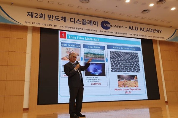
“Semiconductor thin film deposition process, which is the general process that is being used, has reached its limit. ALD (Atomic Layer Deposition) method is the new way to deposit thin films.” said Professor Jeon Hyeong-tak of Hanyang University at the ‘Second MECARO-ALD ACADEMY’ that was held at Hanyang University on the 28th regarding ALD method.
ALD method is seen as the next technology for ‘deposition’ process that is a key process during semiconductor fabrication process. Semiconductor fabrication process begins with the deposition of thin films on a circular wafer one layer at a time. Deposition process is when thin films are deposited one layer at a time. Usually, CVC (Chemical Vapor Deposition) and PVD (Physical Vapor Deposition) methods are used during deposition process. When wafer is placed in a vacuum space where a particular material is injected, a chemical reaction occurs in this vacuum space and on the surface of a wafer and creates a new thin film on top of a wafer. However, much finer and thinner film is soon to be needed as a chip becomes smaller and more integrated.
ALD method has been developed to solve this issue. ALD repeatedly injects ‘precursor’ and ‘reactant’ and induces chemical reaction to occur only on the ‘surface’ of a wafer.
While CVD method deposits thin films as chemical reaction occurs in a vacuum space and on the surface of a wafer, ALD induces chemical reaction to occur only on the surface of a wafer and it can reduce the thickness of a thin film by half. Also, because atoms that are not used for forming an atomic layer is bounced off, thin films with constant thickness can be formed.
Professor Jeon explained that ALD method is already used during many steps of memory semiconductor fabrication process.
“ALD method is used to make a capacitor, which stores and sends data within a DRAM, more detailed and finer.” said Professor Jeon. ““ALD method can also place tungsten, which acts as an electrode even for the lowest layer of a NAND flash memory chip that has more than 96 layers, evenly and meticulously.”
Productivity issue, which is seen as a weak point of ALD method, is also being improved. Although ALD method can form thin films meticulously, it can take quite a long time.
“Batch-type method that forms thin films by putting wafers all together and spatial-type method that forms thin films by moving wafers are being actively developed.” said Professor Jeon.
Applications of ALD method are also being developed. “There are researches done on ALE (Atomic Layer Etching) method that uses atomic layers for etching process and a method where the deposition of atomic layers occurs only on the surface of a desired wafer.” said Professor Kim Woo-hee of Hanyang University.
MECARO-ALD ACADEMY was hosted by the Korean Society of Semiconductor & Display Technology for university students and representatives from the industry who encounter ALD method for the first time. The academy was sponsored by MECARO that has localized precursor material that is absolutely needed for ALD method.
Staff Reporter Kang, Hyeryung | kang@etnews.com