War clouds are starting to form within the memory semiconductor market as Intel is consistently having its eye on Samsung Electronics and SK Hynix that are currently two powerhouses in the market. Intel is the clear powerhouse in the CPU market that plays the role of a brain within a computing device. However, it is looking to reclaim the titles that Samsung Electronics and SK Hynix hold with ‘Optane’ memory. As a result, Samsung Electronics and SK Hynix have become tense. Samsung Electronics’ plan is to distance itself from newcomers by introducing state-of-the-art technology called EUV (Extreme Ultraviolet) process to DRAM. As South Korean companies and American companies that have maintained their positions within the memory semiconductor market and the system semiconductor market respectively, it is expected that there will be new battles within the memory market.
Intel is actually the origin for the development of DRAM after going back to the history of the semiconductor industry. In October of 1970, Intel put out 1KB memory called ‘1103 memory’. This is the start of the history of DRAM.
Intel reduced the number of transistors, which act like a switch within a semiconductor, from its SRAM called ‘1101’ memory that was released in 1969 by one-sixth. While raising the degree of integration but reducing the manufacturing cost, it was able to monopolize the DRAM market.
However, its glory did not go too long within the memory market as Japanese companies had gone after the market in 1972. Major electronic product manufacturers such as NEC, Fujitsu, and Seiko had started to target the semiconductor market. Intel started to lose its ground within the market as Japanese companies had gone after Intel with low-priced products and it ultimately carried out restructuring on its memory business department.
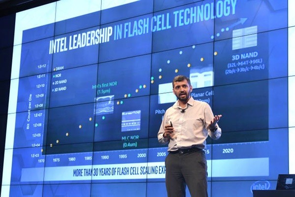
Intel decided to go after the NAND flash memory market in 1988. While it started to grab the upper hand in the market in early 2000s, Samsung Electronics came out with V NAND technology that stacks NAND flash memories vertically and weakened Intel’s influence within the market.
Intel, which had gone through two hardships, has recently decided to go after the NAND flash memory market once again with its ‘Optane memory’ technology.
It announced that it would create a memory based on a completely new concept using 3D XPoint technology that it had worked on for 10 years with Micron Technology. ‘Optane DC Persistence memory’ is the product based on 3D XPoint technology that was introduced by Intel for the first time this year.
According to Intel, Optane memory that is competitive in price is able to supplement information storage ability and appropriate speed when number of DRAMs needs to increase drastically as amounts of information and capacity have increased explosively. Biggest capacity for Optane DC Persistence memory is 512GB that is 8 times bigger than that of 64GB DRAM that is currently the mostly used DRAM.
Intel is planning to target the datacenter market first that is managed by multinational IT companies such as Google, Microsoft, Amazon, and Facebook.
Usually, 8 DRAMs go into single CPU and they help CPU with calculating information. Intel’s goal is to replace 4 of these DRAMs with its Optane memory. Although it will not be possible for Intel to replace all 8 DRAMs with Optane memory due to DRAM’s distinct information processing speed, Intel is looking to solidify its position within the market. Just as Japanese companies had come after Intel with low-priced memories in the past, Intel believes that Optane memory is competitive in price.
Actually, Senior Vice President Rob Crooke of Intel visited South Korea last month and told that Optane memory would be competitive in price.
Industry believes that Senior Vice President Rob hinted that Intel would go after the market by setting the price of Optane memory lower than that of current memories on the market. Some predict that Intel will lower the price of Optane memory even more if the DRAM price falls.
Reason why Intel is trying to go after the memory market once again is because it is looking to change itself as a ‘platform’ company. Its strategy is to create a ‘new Intel inside’ by researching and developing various environments and devices that surround CPU.
“Market shares owned by Samsung Electronics and SK Hynix are not important to us.” said a representative for Intel. “We believe that we will be able to secure a new territory within the market with our Optane technology.”
Industry points out CPU and compatibility as the strengths of Intel. “If Intel continues to put out CPUs that are only compatible with its next-generation memories, it will be able to catch up to Samsung Electronics and SK Hynix soon.” said a representative for the industry.
Samsung Electronics, which is currently the top company within the memory semiconductor market, has become tense as Intel has re-entered the memory market. “Companies that are always putting in efforts and are good at everything are threats to us.” said President Jin Kyo-young of Samsung Electronics Memory Business Department recently regarding the news that Intel has entered the market with Optane memory. “It is necessary for us to listen closely to what our competitors say.”
Samsung is putting in efforts to hold Intel in check to maintain its position within the memory market.
Prime example of its efforts is its collaboration with AMD that is a rising company within the CPU market. In August, Samsung announced its DRAM module that will go into AMD’s 2nd Gen EPYC CPU. Its strategy is to capture its customers’ taste with 256GB memory for server.
“We are closely working with AMD within different areas such as latest processor, memory, and storage that will go into next-generation servers.” said Executive Director Han Jin-man of Samsung Electronics.
Samsung is also trying to separate itself from others when it comes to manufacturing technology. It has recently developed world’s first packaging technology called ’12-layer 3D-TSV’ that can maintain the volume of a product and the capacity of high bandwidth memory (HBM) at the same time. It is planning to introduce EUV process to some of the layers of DRAM in 2020.
Staff Reporter Kang, Hyeryung | kang@etnews.com