South Korea’s semiconductor industry is continuing to put in efforts to improve and to make 3D TSV (Through-silicon via), packaging and FoWLP (Fan-out Wafer-Level Packaging), and FoPLP (Fan-out Panel-Level Packaging) technologies more effective in order to raise the performance of semiconductors and the degree of integration.
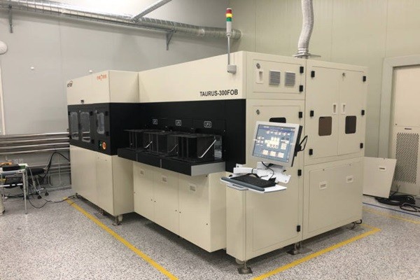
KOSTEK SYSTEM (CEO Bae Joon-ho) has developed a wafer temporary bonder and debonder systems called ‘TAURUS-300FOB (Fan-out Bonder) and ‘TAURUS-300FOD (Fan-out Debonder) that are for semiconductor fan-out packaging process and can be applied to both FoWLP and FoPLP technologies and it has supplied both of the systems to South Korean companies. Because South Korean companies had depended on foreign companies for these systems in the past, KOSTEK SYSTEM is expecting a huge import substitution effect in the future.
Its wafer temporary bonder and debonder systems can be used during a fan-out packaging process.
TSV packaging process grinds the back of a device wafer (back-grinding), creates holes that penetrate through a chip, and lays out copper wiring to stack many chips. During this process, carrier wafer that supports device wafer to prevent device wafer from bending is attached on the front of device wafer with either liquid or film-type temporary adhesive. This is when a bonder system is used to attach carrier wafer. Carrier wafer can be detached when wiring and bumping processes are completed after grinding the back of device wafer.
Fan-out packaging process replaces a completed chip in a circular or square-like shape and takes out copper wiring out of a chip. However, wafer warpage problem can occur during an epoxy molding process. As a result, carrier wafer is bonded on the back of wafer to remove warpage problem and is removed after wiring and bumping processes are completed.
KOSTEK SYSTEM has developed many key technologies such as alignment technology so that two wafers are identical, technology that can evenly distribute pressure that is applied to wafers during bonding process, technology that maintains the thickness of a wafer, and technology that prevents empty space such as bubble when film is attached to a wafer. It has also applied for patents on many relevant technologies and registered them.
This bonding technology can also be applied to micro-LED display manufacturing process.
Bonding process needs to be performed on a wafer to manufacture small micro-LEDs whose sizes are between 10 and 100 micrometers. Carrier wafer needs to be bonded followed by follow-up patterning process.
This bonding technology can also be used for chip transfer process that is the most difficult and expensive process during a micro LED manufacturing process. Because it can transfer hundreds of thousands of micro-LED chips at once, it can drastically reduce the manufacturing cost.
Wafer temporary bonder and debonder systems that are currently used by South Korean semiconductor manufacturers for their 3D chip and interposer manufacturing lines come from foreign companies. Companies from Germany, Japan, and Austria currently dominate the market. Because TSV bonder and debonder systems cost $10 million and are very important during a semiconductor manufacturing process, there will be huge import substitution effect once KOSTEK SYSTEM supplies its systems on full-scale.
KOSTEK SYSTEM is using film-type adhesive for its two new systems. It is also developing a system based on liquid adhesive and it is planning to verify credibility of this system with South Korean companies.
“Not only our systems can replace foreign systems that are currently used, but they can also be applied to both FoWLP and FoPLP processes and they can also be applied to TSV packaging and micro-LED packaging processes in the future.” said a representative for KOSTEK SYSTEM.
Staff Reporter Bae, Okjin | withok@etnews.com