Samsung Electronics has also secured semiconductor packaging technology that will distance itself further from its competitors. It developed ’12-layer 3D TSV (Through-silicon via)’ technology that increases the capacity of a memory while maintaining the size of a chip.
Samsung Electronics announced today that it has developed the industry’s first 12-layer 3D-TSV technology. This technology stacks and interconnects 12 DRAM chips that have the thickness of less than half of the thickness of a paper so that they can exchange electric signals with each other.
This technology is mostly used for packaging HBMs (High Bandwidth Memory). Unlike current DRAMs, HBM is directly attached to the side of a CPU or a GPU and helps with processing information. Its major role is to reduce power consumption and increases operation speed of a CPU. As a result, next-generation HBM needs to implement high capacity even through limited chip size.
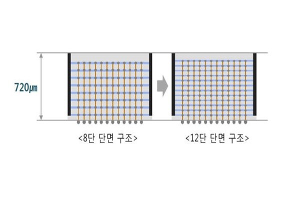
8-layer 3D-TSV was the highest number of layers until Samsung Electronics has come out with 12-layer 3D-TSV technology. Through 12-layer 3D-TSV technology, capacity of a HBM is now increased by 1.5 times while the size of a chip remains the same.
Samsung Electronics announced that it has maintained the thickness of the package (720µm) although it has increased the number of layers by four more layers. This is because Samsung Electronics applied a method that reduces the thickness of a DRAM chip by less than half of the thickness of a paper (100µm). Strengths of a HBM are maximized when the size of a chip becomes smaller as HBM is attached right next to major operation processing devices.
“Our customers will be able to release products with higher performance and higher capacity without changing much of their design.” said a representative for Samsung Electronics.
Samsung Electronics has maintained the strengths of 3D-TSV technology that creates holes for electrons, which are one-twentieth of the thickness of a single strand of human hair, at the top and the bottom of a chip. This technology can greatly improve power consumption, information processing speed, and chip size than packaging (wire bonding) by connecting many wires outside of a semiconductor.
Although there needs to be more holes as there are more layers, Samsung Electronics explained that it has implemented smooth exchange of electric signals by having more than 60,000 holes per product.
Samsung Electronics is planning to continue to become the leader within premium semiconductor markets by supplying high-capacity HBMs based on 12-layer 3D-TSV technology at the right time and according to the demands of its customers.
“State-of-the-art packaging technology is becoming more important in areas such as AI, autonomous driving, and HPC (High-Performance Computing).” said Vice-President Baek Hong-joo of Samsung Electronics’ DS Division. “We are going to maintain our leadership even in semiconductor packaging field through 12-layer 3D-TSV technology.”
Meanwhile, Samsung Electronics has been making efforts such as acquisition of Samsung Electro-Mechanics’ PLP (Panel Level Package) business into expanding its packaging business. Vice-Chairman Lee Jae-yong of Samsung Electronics visited a semiconductor back-end process line in Onyang in August and examined current state of chip assembly process.
Staff Reporter Kang, Hyeryung | kang@etnews.com