Samsung Electronics Foundry Business Department has set up a plan to go straight to 6-nano process based on 7-nano process. This is its strategy to counterattack Taiwan’s TSMC as it took a supply of 7-nano chips from major customers such as Qualcomm and others that are consigned.
Although 6-nano process is based on 7-nano technology, width of electrical wiring is much thinner. It is expected that 6-nano process will be more advantageous than 7-nano process in terms of production cost due to smaller areas of chips. Electric efficiency and performance will be improved as well.
Samsung Electronics has set up a goal to mass-produce 6-nano chips by 2019. It is planning to respond to amount of 7-nano chips that it lost to TSMC with 8-nano process, which is a minor upgraded version of 10-nano process.
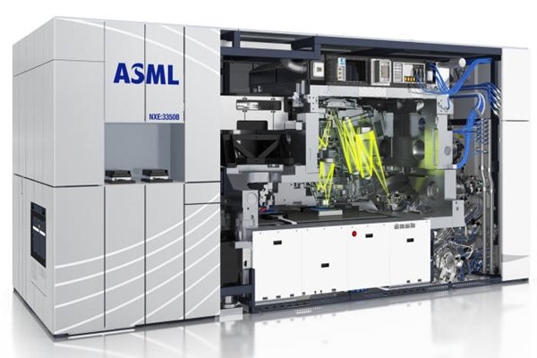
According to related industries on the 26th, Samsung Electronics Foundry Business Department realized that it is too late to secure customers for 7-nano process as many of them already chose TSMC and has decided to focus all of its capabilities into 6-nano process. It has decided to bring in 2 ASML NXE3400B, which is a next-generation EUV (Extreme Ultraviolet) stepper, this year and 7 next year. One of this equipment will be placed at its 17 line, which is located in Hwasung, Gyeonggido, shortly while the other one will be brought in during second half of this year. It is expected that 7 ASML NXE3400Bs that will be brought in next year will replace previous equipment that are set up at 7-nano and 6-nano system semiconductor foundry production facilities.
TSMC minimized its resources that are spent to develop 10-nano process and went straight to 7-nano process. From its 10-nano process, it only produces chips for Apple’s next iPhones. Through this strategy, TSMC took a supply of Qualcomm’s early 7-nano chips that are consigned from Samsung Electronics.
Samsung Electronics believed that calculations of earnings and experiences are not from an aspect of production cost if it produces 7-nano chips through current exposure equipment. Exposure is an important semiconductor process that engraves circuit patterns. Experts in semiconductor production also believe that Samsung Electronics can reduce production cost and areas of chips by utilizing EUV equipment from parts of 7-nano process. Because light wavelength of EUV is short (13.5nm), it can engrave 7-nano circuit pattern at once and this is why Samsung Electronics has decided to bring in next-generation exposure equipment to its 7-nano mass-production lines.
TSMC’s first 7-nano process does not use EUV equipment. It instead uses immersion equipment with higher limit of resolution by utilizing ArF (Argon Fluoride) excimer laser that has light wavelength of 193nm and immersion technology. If EUV equipment is not used during 7-nano process, quadruple patterning technology that performs multiple exposure process needs to be applied on certain processes. This process increases production cost due to longer process time. TSMC is planning to commercialize its first 7-nano process next year and is planning to use EUV equipment during its second 7-nano process. Its goal is to mass-produce 7-nano chips in 2019. TSMC, which has gained new customers by quickly commercializing 7-nano process through its current exposure equipment, is planning to prevent breakaway by using EUV equipment in the future while emphasizing ‘true 7-nano process’.
Samsung Electronics is going to focus all of its abilities and capabilities into 6-nano process while TSMC is focused on 7-nano process. 6-nano process has to be based on 7-nano technologies. Samsung Electronics is planning to mass-produce one type of Exynos chips through 7-nano process and have 6-nano process as its main process.
“Samsung Electronics once got results from skipping over 20-nano process and going straight to 14-nano process in the past and TSMC also gained upper hands in early markets for 7-nano process as it skipped over 10-nano process.” said a high-ranking official in a semiconductor industry. “As Samsung Electronics purchased many EUV equipment, it is expected that Samsung Electronics and TSMC will have fierce competitions with each other in order to secure supplies from their customers.”
Staff Reporter Han, Juyeop | powerusr@etnews.com