South Korean semiconductor package company called NEPES has succeeded in commercializing high-tech FO-PLP (Fan Out - Panel Level Package) technology. This is a very meaningful result as it was able to commercialize this technology faster than any other global companies. Samsung Electro-Mechanics is currently developing PLP technology with a goal of commercialize it during second half of this year.
According to industries on the 14th, NEPES started mass-producing packages this month by applying its PLP technology to a company that produces analog semiconductors for Smartphones. NEPES established mass-production system by converting its Cheongju Campus’s equipment that is related to LCD TSP (Touch Screen Panel) into equipment for producing semiconductor PLP. It had been developing PLP technology for past year in secret.
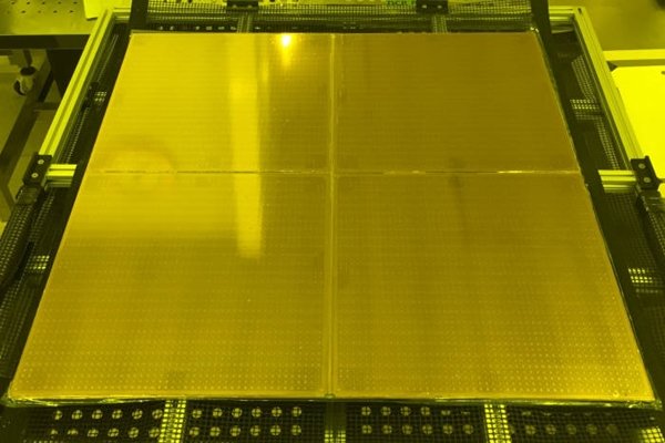
Production efficiency of PLP is higher than WLP (Wafer Level Package). While WLP carries out rewiring process after placing a chip, which is made by cutting a manufactured wafer, on top of circular substrate, PLP carries out its process by placing a chip on top of a quadrilateral supporting substrate. Because it has quadrilateral shape, amount of substrate that is thrown away is less than circular substrate. Package at a lesser cost than WLP is possible if yields are secured.
Products of a company, which has NEPES in charge of packaging through PLP technology, will be shipped to markets as separated products that are applied with Fan In technology and Fan Out technology respectively. Fan Out is a technology that increases number of I/O (Input/Output) by pulling out I/O terminal wiring outside. When this technology is used, it is possible to package high-performance chips with many I/O at a lower production cost. It is also possible to reduce additional production cost since this technology does not need PCB (Printed Circuit Board) for packaging and it can also reduce thickness of final package. TSMC, which is a Taiwanese foundry company, was the first one to commercialize Fan Out technology. Application processors (AP) of Apple’s new iPhones will be packaged through TSMC’s Fan Out technology called InFO (Integrated Fan Out) technology.
“It is more difficult to implement PLP technology than WLP technology and Fan Out technology than Fan In technology.” said a representative for an industry. “NEPES is the first one to converge and commercialize a technology that combines both technologies.”
NEPES is expanding its business with a goal of attracting variety of new customers through FO-PLP technology. Semiconductor companies that deal with RF (Radio Frequency), analog, analog-digital mixed signal, and PMIC (Power Management Integrated Circuit) are its potential customers.
“PLP can greatly reduce production cost.” said Department Head Kim Nam-cheol of NEPES Semiconductor Business Department. “Changes in dynamics of package markets are expected through commercialization of this technology.”
NEPES is planning to increase its sales from package business through its current WLP package technology and new PLP technology.
Samsung Electro-Mechanics, is accelerating its preparation for mass-production by establishing PLP line in Cheonan. It seems that first product will be PMIC and it is planning to expand and apply PLP technology to memory and AP in the future. Industries predict that actual commercialization will take place next year.
Staff Reporter Han, Juyeop | powerusr@etnews.com