A research team from South Korea has developed transparent semiconductor material that can be easily bent. It is expected that this material will be used for variety of portable devices and greatly contribute in developing future semiconductor devices.
National Research Foundation of Korea (Chairman Cho Moo-jae) and a research team led by Professor Lee Gwang-hee of Gwangju Institute of Science and Technology (GIST) made an announcement on the 5th that they have succeeded in developing flexible and transparent organic semiconductor material by mixing polymeric semiconductor with insulating polymer.
So far no semiconductor material has both flexibility and high transmittance of visible ray. Semiconductor materials such as metallic oxide and carbon materials as well as silicon that is being mostly used currently also do not have both characteristics.
Even polymeric organic semiconductors, which are receiving spotlights for their flexibility, have difficulty in securing transparency due to their characteristic of absorbing visible ray. Although semiconductors can be transparent if they are made up of thin films, semiconductor’s characteristics such as mobility of charge can be weakened.
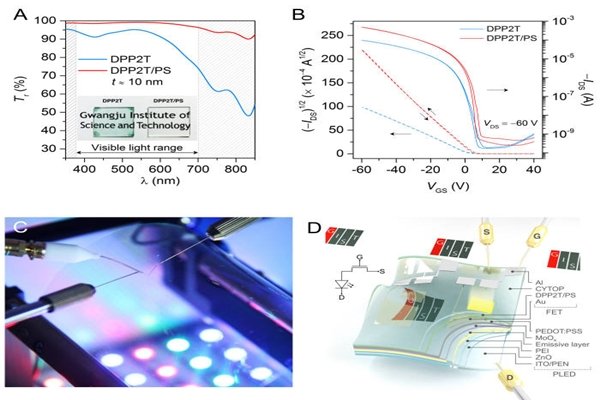
Research team added polymeric polystyrene as an insulator to small amount of polymeric semiconductor (DPP2T). DPP2T forms thin net-like structure within transparent interior of polystyrene. Transmittance of visible ray can be close to 100% as this material is made up of a structure that fills large holes with minimal passageways. Object that is placed on the other side can be seen without any distortion in color through a thin film.
Performance of mixed net-like semiconductor is more superior compared to pure thin-film DPP2T. Although actual area where charges move is only 15% of current material, mobility of charges is improved by almost 4 times. Charges move effectively along polymeric chain that is created by net-like structure.
Semiconductor process is also very simple which is advantageous in mass-production. Research team explained that semiconductors can be mass-produced easier and faster by utilizing ‘solution process’ that imprints materials by mixing each material into a solvent.
This material is expected to push forward development of new electronic devices such as transparent body signal monitoring system that can be attached on a human body, aesthetically outstanding wearable devices, and ultra-thin transparent and flexible displays.
“We have implemented functions that everyone have dreamed of by surpassing possibilities that organic electronic materials possess.” said Professor Lee Kwang-hee. “By establishing a new technical paradigm, we are able to fulfill technologies that seemed impossible in the past.”
Staff Reporter Kim, Youngjun | kyj85@etnews.com