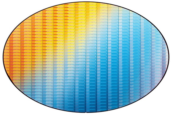
Samsung Electronics and TSMC are competing each other in introducing Gen.3 14 and 16-nano FinFET system semiconductor processes and they are focusing on reducing amount of electricity consumption and production cost.
During IR to present yearly result for 2015, TSMC made an announcement that it is planning to enter mass-production system of chips produced by 16-nano FinFET Compact (FFC) process sometime during 1st quarter of this year. TSMC had finished developing 16-nano FFC process in 4th quarter of last year. Co-CEO C.C Wei of TSMC explained that 16-nano FFC process focuses on reducing production cost more than before and implementing low electricity.
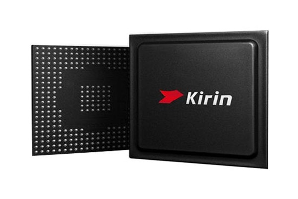
TSMC made an announcement of its first 16-nano FinFET (FF) process at the end of 2014 and secured Huawei’s affiliate called HiSilicon as its first customer. HiSilicon’s Kirin 950 that is used for Huawei’s premium Smartphone called Mate 8 is produced by TSMC’s 16-nano FF process. It is heard that A9 Chip, which is used for Apple’s iPhone 6S series, is mass-produced by 16-nano FinFET Plus (FF+) process that was announced in early 2015. By adding FFC process, TSMC now has total of 3 16-nano processes.
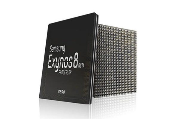
Samsung Electronics recently had succeeded in mass-producing Gen.2 14-nano FinFET process called LPP (Low Power Plus) that ha 15% lesser electricity consumption compared to Gen.1 14-nano process called LPE (Low Power Early). Exynos 8 OCTA series that is used for Galaxy S7 and Qualcomm’s Snapdragon 820 are mass-produced by Samsung Electronics’ 14-nano LPP process. Just like TSMC, Samsung Electronics is also preparing for Gen.3 14-nano FinFET process.

“We are going to develop a derivative process that will follow Gen.2 14-nano process and lead mobile chip and foundry markets.” said Vice-President Bae Young-chang of Samsung Electronics’ System LSI Business Department’s Strategy Marketing Team.
Unlike 32-nano and 20-nano processes, it seems that 14 and 16-nano processes will become ‘longevity’ processes because it has become difficult to reduce line width as processes are entering 10-nanos. If it is not easy to secure yields, then it is going to lead to increase of cost for production of chips. This is why 28-nano process is still the main process after long years.
Even if Samsung Electronics and TSMC finish developing 10-nano process at the end of this year and enter mass-production system next year, only Apple, Qualcomm and few other will be able to produce related chips. This is the reason why they have no choice to continuously upgrade their current 14 and 16-nano processes.
“It is predicted that Samsung Electronics and TSMC will develop Gen.3 14 and 16-nano derivative processes and focus on securing customers before they finish developing high-tech 10-nano process at the end of this year.” said a representative of this industry. “Even if 10-nano process is commercialized, there still will be many fabless businesses that will use 14 and 16-nano processes that cost relatively cheaper.”
Staff Reporter Han, Juyeop | powerusr@etnews.com