Samsung Electronics is speeding up its 10 nm-level foundry business and it is enhancing its current 14-Nano process. It is also raising transference number and chip function and mass-produces 10-Nano FinFET in end of next year.
Samsung Electronics started recently on its operation to enhance current 14-Nano process. It is essential to change chip design while maintaining current production facilities.
It is possible to raise chip function by one level if current process is enhanced. By decreasing electricity consumption level, electronic efficiency is increased and data processing speed is improved. Compared to 20-Nano process, electricity consumption of 14-Nano is decreased by 35% and its data processing speed is increased by 20%.
Industry is predicting that chip function can be similar to 10-Nano level if processes are enhanced. It is heard that competitor TSMC’s 16-Nano FinFET Plus Process Foundry’s function is similar to that of Samsung Electronics’ 14-Nano. If enhancement is finished, Samsung Electronics can produce chips with better functions while having similar processes with its competitors.
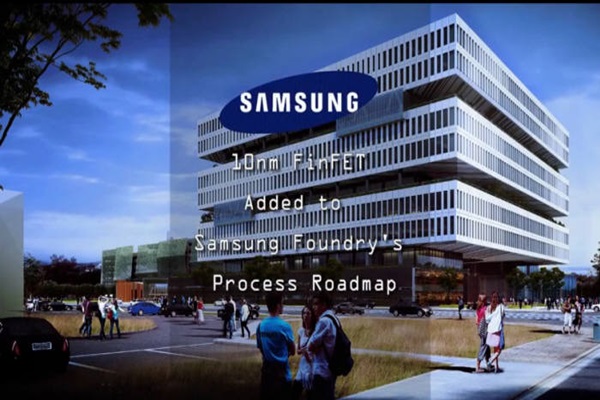
It also formulated timing to mass-produce 10-Nano process. Samsung Electronics’ corporate body recently announced that it will add 10-Nano FinFET Manufacturing Process to foundry mass-producing plan, which will happen in end of next year.
Samsung Electronics recommended mobile, consumer, network, and server chip manufacturers to use 10-Nano process in their developments for next-generation products. It also stressed that it is supporting Multi-Project Wafer (MPW).
MPW signifies that many chip design projects to be put into a sheet of wafer. Generally it is expensive to test if chip is designed well to apply one chip project on to a sheet of wafer. If a sheet of wafer is shared, cost can be reduced while it is also enough to manufacture samples or test chips.
Samsung Electronics stressed that it is supporting MPW and is leading chip manufacturers to design based on 10-Nano process.
Industry interpreted that Samsung Electronics chose a strategy to operate both production lines rather than changing current 14-Nano facility to 10-Nano due to cost because rate of return compared to investment is not that big to change 14-Nano facility in which Samsung Electronics invested billions of dollars (trillion KRW) into to 10-Nano process. Including Exynos Mobile Application (AP), it secured Qualcomm, Nvidia, and etc. as its customers, but there is not enough rate of return. It is very dangerous that TSMC, which fell a step behind in competition for 14-Nano, is speeding up its 10-Nano process. Samsung Electronics cannot delay its investment in mass-producing 10-Nano.
“Even if Samsung Electronics produces chips with 10-Nano-like functions at 14-Nano line, it can be seen on surface as if Samsung Electronics gave the lead to its competitor if TSMC succeeds in mass-producing 10-Nano process. Although it is not an appropriate time to collect enough investment of 14-Nano process, it is why it cannot delay its investment in mass-producing 10-Nano process.” A person in semiconductor industry said that 10-Nano process is very important to Samsung Electronics if it wants to compete against TSMC.
Industry is interested in what kind of competition structure will Samsung Electronics’ 10-Nano-based next-generation Exynos Chip will form with Qualcomm’s Snapdragon because number of sales of Exynos 7420 increased as TSMC had a terrible experience with problems of Qualcomm’s Snapdragon 810’s functions that were produced in 20-Nano process.
Staff Reporter Bae, Okjin | withok@etnews.com