Starts Mass Production in 2017
Samsung invests 14.26 billion dollars(USD, 15.6trillon KRW), which is the all-time biggest investment in single semiconductor product line.
Pyeongtaek City Gyeonggi-do Province is getting ready to be born as ‘Samsung Semiconductor Valley’, which is going be set as an advanced base for next 40 years and have the biggest product line in the world built. 14.26 billion dollars are going to be invested, which is the all-time biggest investment for a single semiconductor product line and it is going to be in operation from 2017. Samsung is completing a high-tech semiconductor product line by having bases in Giheung, Hwaseong, and Pyeongtaek.
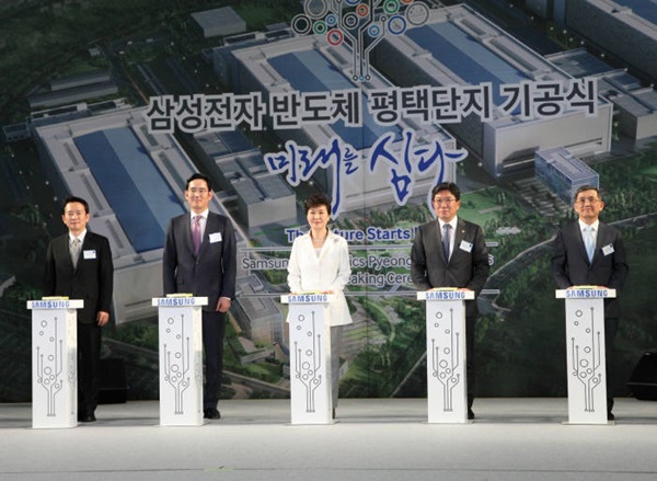
Samsung Electronics held ‘Samsung Electronics Semiconductor Pyeongtaek Complex’ ground breaking ceremony at Godeok Urban Innovation Corporation industrial complex on the 7th and it started its product line construction. 600 people including President Park Gunhye, Minister of Ministry of Trade, Industry & Energy Yoon SangJik, Governor of Gyeonggi-Do Nam Kyeongpil, Mayor of Pyeongtaek Kong Jae-Kwang, Vice-Chairman of Samsung Electronics Lee JaeYong, Representative of Samsung Electronics Kwon OhHyun, and clients attended this ceremony.
Pyeongtaek semiconductor complex, which has the area of 400 soccer fields and a site area of 2,892,561 ㎡ is constructed as Korea’s biggest semiconductor production complex. It is almost equal to the sizes of existing production complexes in Giheung and Hwaseong put together.
Samsung Electronics is constructing a first semiconductor product line by investing 14.26billion dollars as a first step by 2017, which is the biggest investment for a single semiconductor product line. It’s been almost 3 years since Samsung Electronics invested such great equipment investment since it invested in semiconductor 17 line establishments in Hwaseong in 2012. Investment was finalized a year earlier than an original plan, which is President Park Gun Hye administration’s 3 year innovative economy plan that plans to revive local economy. Increased demands from small semiconductor Equipment Company are highly anticipated.
Samsung semiconductor complex has been around for 40 years and now it is preparing for the next 40 years by having Pyeongtaek semiconductor complex as its advanced base. Having being the best in world semiconductor market as a goal, Samsung chose Pyeongtaek to speed up the gap in technology, which puts memory and non-memory together, between Samsung and other competitors.
If Pyeongtaek line starts mass-producing in 2017, it will become the biggest semiconductor cluster that connects Giheung, Hwaseong, and Pyeongtaek. Pyeongtaek complex will be a core that builds ICT valley that connects metropolitan area and Chungcheong by being in the middle of Samsung’s ICT R&D center and display production complex in Cheonan and Asan area.
Samsung Electronics is planning to have Pyeongtaek as a nucleus that will lead semiconductor market for 40 years by building in high-tech process. It is planning to mass-produce D-Ram that is built by high-tech process, and have a system semiconductor product line that can fight for preoccupancy in loT market.
Government and Samsung Electronics is predicting that Pyeongtaek semiconductor complex will affect the economy by creating employments for 150,000 people and causing 40 billion dollars from production. Materials, facilities, and front back industries will contribute to revitalization of Korea’s economy.
Domestic and foreign industries are very curious about what process and products will be used and produces in Pyeongtaek complex by Samsung Electronics. Although D-Ram by 20-nano process is quickly changing and gaining much importance, it is possible that D-Ram by 10-nano level process will be used if Pyeongtaek line were to start mass production after 2017.
It is predicted that high-tech process will be reviewed in a system semiconductor because they will start mass producing 10-nano finFET starting end of next year.
“Samsung is showing a mentality of an enterprise by not being satisfied with the growth and investing for competitiveness in the future. I wish that Samsung becomes the center of world’s semiconductor production and worthy of its name.” President Park Gun Hye said about Samsung’s investment in Pyeongtaek semiconductor complex.
“It was considered as a rash move when South Korea started a semiconductor business 40 years ago, but we became the best in memory industry within 10 years and we are still the best for 22 years.” Kwon Oh Hyeon Samsung Electronics Vice-President said about a history of semiconductor business in South Korea. “Pyeongtaek semiconductor complex is a new challenge for next 40 years in semiconductor business, and we will once again leap forward into this challenge to fulfill our desire to be the best semiconductor business in the world.”
Senior Reporter, Kwon Sanghee | shkwon@etnews.com,
Staff Reporter, Bae Okjin| withok@etnews.com