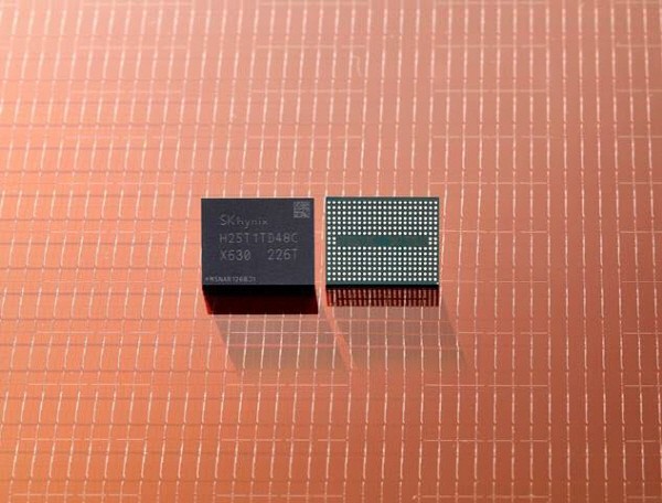
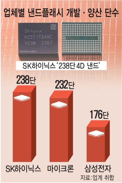
SK Hynix has successfully developed the world's most advanced 238-layer NAND flash storage chip. It surpasses the technology in Micron's recently announced 232-layer. SK Hynix unveiled their 238-layer 512 gigabit (Gb) TLC 4D NAND sample at the 'Flash Memory Summit' held in Santa Clara, United States on the 3rd and announced that it will start mass production in the first half of next year. This is the culmination of 1 year and 7 months of development of 176-layer NAND in 2020. A key feature of NAND is that it is the world's smallest in size yet also the most advanced. NAND flashes have higher capacity depending on the number of stacks in the same space.
The data transfer rate of the 238-layer NAND flash is 2.4 Gb per second. It is 50% faster than the previous generation. NAND flash is divided into SLC (1 cell), MLC (2 cells), TLC (3 cells), and QLC (4 cells) depending on how much information is stored in one cell. More data can be stored in the same area as the memory space increases. SK Hynix's 238-layer NAND had adopted the TLC standard.
A four-dimensional (4D) structure is implemented into the chips. 4D reduces cell area per unit which results in higher production efficiency, compared to 3D. SK Hynix has been introducing 4D products that surpass existing 3D since their 96-layer NAND developed in 2018. SK Hynix applied technologies such as CTF, which solves cell interference problems, and PUC, which increases production efficiency by changing circuit layout for 4D implementation. The energy consumption of the chip to read data has been reduced by 21%. The company explained that it has also accomplished environmental, social and governance (ESG) performance by reducing power consumption.
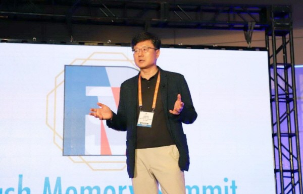
Jeong-dal Choi, vice president of NAND development at SK Hynix, said, “We have secured global top-tier competitiveness in terms of cost, performance and quality by introducing the 238-layer product, which was developed using 4D NAND technology,” and emphasized that, “We will continue to innovate in order to break through the technological limits."
SK Hynix will first supply 238-layer products used in client solid-state drives (cSSDs) for PC storage devices. Afterwards, it will expand the range of products to include high-capacity SSDs for smartphones and servers. Next year, it will also introduce a 1 terabit (Tb) product with double the capacity of the current 512 Gb.
By staff reporter Dong-jun Kwon djkwon@etnews.com