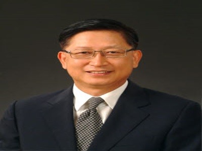
NEPES has brought in Chung Chil-hee, who used to work as an advisor and the president of Samsung Advanced Institute of Technology (SAIT) successively, to be the new chairman of the company.
According to the industry, NEPES has appointed Chung Chil-hee, who used to work as an advisor at Samsung Electronics, as the new chairman.
A representative for NEPES explained that Chairman Chung is overseeing the company’s semiconductor business.
Chairman Chung is one of main leaders who are responsible for making Samsung Electronics’ semiconductor business what it is today. Since joining the company in 1979, he had held different positions. When he became the president of SAIT, he was responsible for development of Samsung Electronics’ future technologies such as quantum dot and neural processing. In addition to holding the president position of SAIT, he had also held a variety of positions such as an advisor at SAIT, the chairman at Nano Technology Research Association, and a member of the Presidential Advisory Council on education, Science & Technology.
NEPES, which was established in 1990 by Chairman Lee Byung-koo, is a company that specializes in semiconductor packaging process. During the company’s early days of establishment, it established a steppingstone for growth by commercializing developing solution and coating solution that are used for semiconductors and displays. In early 2000s, the company started working on bumping process that is part of semiconductor packaging process. It has now become a company that specializes in packaging process with advanced packing process technologies such as WLP (Wafer Level Package), FOWLP/PLP, and SiP (System in Package).
NEPES is likely to have brought in Chairman Chung Chil-hee, who is a semiconductor expert, in order to strengthen the company’s growth and capabilities as semiconductor technologies continue to be more advanced at a rapid rate. Normally, semiconductor packaging involves protecting a semiconductor from external impact or connecting an external device to the chip. It is part of the semiconductor back-end process.
However, there has been a tendency recently where such boundary may fall apart. As packaging has proven to have an effect in improving semiconductor’s performance, there has been development of advanced packaging technologies that connect external devices to chips during front-end process.
In order to keep up with the trend and strengthen its capabilities in packaging continuously, it is likely to have brought in a semiconductor expert to be the next chairman.
South Korea’s semiconductor industry has recently started to experience a growth in the foundry market with Samsung Electronics at the center. Because the growth in the foundry market is leading to bigger semiconductor packaging market, NEPES is expected to have a bigger role in the packaging market.
NEPES’ overall business is made up of semiconductor, electronic materials, and rechargeable battery. Out of these three sectors, the semiconductor sector occupies the highest percentage of the company’s sales.
Staff Reporter Yun, Geonil | benyun@etnews.com