Samsung Electronics has begun making preparations for a large-scale memory semiconductor investment. It is reported that the company is planning on a plant and equipment investment for monthly production capacity of 100,000 12-inch wafers in the first half next year alone. This move shows the company’s intention to actively respond to recovery of the global economy after the COVID-19 pandemic and lead the global market. It also shows that the company, which is the world’s biggest memory semiconductor maker, is close to implementing a “super-gap” strategy.
According to the industry on Wednesday, Samsung Electronics plans to make such investment in the first half next year. It is reported that the company recently shared its investment plan with semiconductor equipment makers and is working on adjusting detailed schedules with them.
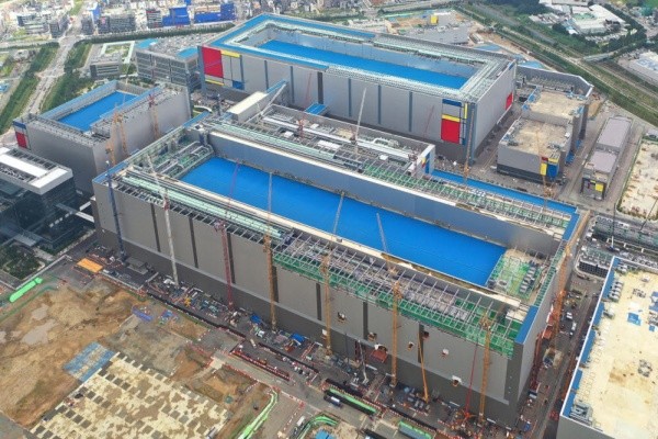
The company plans to split the investment evenly for DRAM and NAND flash. A portion of the investment for DRAM will be centered around the Pyeongtaek Line 2 (P2) while the other portion for NAND flash will be spread out amongst the company’s plant in Xi’an and P2.
Monthly production capacity of 100,000 wafers is equivalent to that of Samsung Electronics’ single memory fab. Production capacity of the company’s first plant in Xi’an, which was built with an $10.8 billion investment, is 100,000 12-inch wafers. Also, because production capacity of the P2 fab when it is packed with facilities and equipment is 200,000 12-inch wafers, production capacity of 100,000 wafers can be seen as a significant amount. Because the company is looking to make the investment in the first half next year alone, it can be seen that the company is looking to accelerate its investment in memory facilities.
The reason why Samsung Electronics is making an aggressive approach towards memory facilities because it believes that the forecast of the global memory semiconductor market is very bright.
Although demands for semiconductors had been rising rapidly due to a rise in contactless economic activities resulting from the spread of COVID-19, semiconductor prices have slowed down a bit as major data center companies such as Google and Amazon started to manage their inventories for memories in the second half.
During a conference for third quarter performance, Samsung Electronics announced that both ASPs (Average Selling Price) of DRAM and NAND flash dropped around 10% compared to the second quarter.
However, it is reported that multinational data center companies recently started to use up their inventories again. In other words, the companies have resumed making investments in memories for servers. Because the global smartphone market, which has shown a negative growth this year, is also expected to recover next year, Samsung Electronics is planning on an intensive investment in a short period of time.
“Although there is a great chance that data center companies will continue to adjust their inventories of DRAMs until the end of this year, there can be a short supply in the second half next year as data center companies begin stocking up inventories again and as demands for smartphones start to recover.” said Kim Young-woo who work as an analyst for SK Securities.
Policies by countries to revitalize their economies are also positive for the future of the global semiconductor market. “While the growth rate of the global GDP fell 4.5% this year, next year’s GDP is likely to be around $87.54 trillion that is a 4.8% jump.” said a semiconductor market researcher IC Insights. “We plan to make an upward adjustment to the global semiconductor market’s forecast in 2021.”
It is likely that Samsung Electronics is preparing a large-scale investment in order to solidify its lead in the global semiconductor market based on these predictions.
Regarding the investment for next year, Samsung Electronics announced that no detailed plan has been decided yet.
Staff Reporter Kang, Hyeryung | kang@etnews.com & Staff Reporter Yun, Geonil | benyun@etnews.com