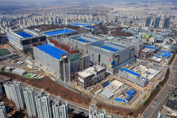
The size of South Korea’s semiconductor “testing house” is growing along with a growth of Samsung Electronics’ system semiconductor business. Semiconductor testing companies such as NEPES Ark, LB Semicon, and Tesna, and Hana Micron are dealing with increased supplies of system semiconductors by making investments in necessary facilities and equipment. Some within the market believe that there needs to be an all-around national support that even reaches the back-end ecosystem in addition to the semiconductor design and foundry fields in order to continue to develop the nation’s system semiconductor ecosystem.
According to the industry on Thursday, LB Semicon that is well known as an outsourced semiconductor assembly and test (OSAT) company recently announced its plan to make a $49.7 million (58.1 billion KRW) investment in facilities and equipment. It announced that its investment will be used to build additional testing facilities for CMOS (Complementary Metal Oxide Semiconductor) image sensors and system on chips (SoC).
LB Semicon primarily focuses on bumping process that hangs “metal balls” at the bottom of a semiconductor chip and connects the chip to an external connecting terminal. It seems that the company is making the investment in order to deal with increased demands from Samsung Electronics regarding testing on image sensors. “It seems that LB Semicon’s additional facilities and equipment will go into operation in the first quarter next year at the earliest.” said a spokesperson from the industry.
Revenue of Tesna, which has established testing facilities that are most equipped for Samsung Electronics’ image sensors, is also rising at a fast rate. It invested $23.2 million (27.1 billion KRW) last October in order to increase its production capacity. The industry predicts that booming will continue next year as Tesna is preparing to make a similar amount of investment next year. “Our last year’s investment was to build testing facilities this year for image sensors and systems on a chip in a 7 to 3 ratio respectively.” said a spokesperson for Tesna.
NEPES Ark, which was established in April last year as a subsidiary of NEPES, is also building testing facilities based on an $51.3 million (60 billion KRW) investment. Starting from this fourth quarter, it is going to provide a testing service to his major customers for their application processors (AP) based on its own technologies and fan-out panel level package (FOPLP) and wafer level package (WLP) technology of NEPES. It plans to expand its testing service towards radio frequency (RF) chip in the future.
Hana Micron has been investing about $38.5 million (45 billion KRW) since last year in order to secure testing facilities and equipment and started operating the facilities and equipment in January. It has recently been testing Samsung Electronics’ APs for mobile and household uses, 5G RF chips, and power management integrated circuits (PMIC). The operation rate of its plant, which had slowed down a bit in the first half due to COVID-19, has been recovering at a rapid rate since July.
Semiconductor testing process separates acceptable products from defective products in various conditions.
Recent investments by the four testing companies are related to increased supplies of system semiconductors from Samsung Electronics. Samsung Electronics has been increasing product lines of various system semiconductors such as PMIC, RF chip, image sensor, and AP in order to become the top system semiconductor manufacturer by 2030.
As Samsung Electronics increases supplies of these products, South Korea’s semiconductor testing market is also growing naturally. Relationship between Samsung Electronics and these four companies is becoming more like the steady system semiconductor system in Taiwan.
Testing companies such as KYEC, Sigurd Microelectronics, and Ardentec have established relationships with TSMC and are supporting TSMC. In case of KYEC that has about 70% of its revenue coming from testing on wafers and packaging, it made more than $855 million (1 trillion KRW) in revenue alone last year and has significant influence on the industry in Taiwan.
The four testing companies in South Korea mainly test chips that are designed by Samsung Electronics’ System LSI Division and manufactured by Samsung Foundry. It is expected that they will expand their testing as Samsung Foundry obtains projects from outside customers and manufactures various products and continue to make a huge growth as a result.
Such virtuous cycle will require continuous interests and investments from the South Korean Government on the back-end ecosystem of the system semiconductor industry.
“There has to be a structure where foreign IT companies assign orders to Samsung Foundry and packaging and testing are done by South Korean companies.” said a representative for the industry. “In order to maintain benefits of the expansion of Samsung Foundry, the semiconductor back-end industry in South Korea also needs to gain competitive edge just like Taiwanese testing companies.”
Staff Reporter Kang, Hyeryung | kang@etnews.com