Samsung Electronics and SK Hynix are looking to start a new era of semiconductor manufacturing process. While Samsung Electronics is planning to mass-produce the industry’s first “Gate-All-Around (GAA)”, SK Hynix is getting ready to manufacture DRAM based on the extreme ultraviolet (EUV) process. GAA and EUV DRAM are core technologies that will lead the global system semiconductor (foundry) and DRAM markets respectively. Once they succeed in commercializing GAA and EUV DRAM, the gap between South Korea and other countries and the status of South Korea’s semiconductor industry will be widened and elevated even more.
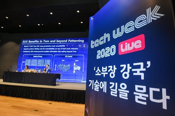
Samsung Electronics and SK Hynix announced their strategies on these next-generation semiconductor technologies on the first day of “Tech Week 2020 LIVE” that began on Wednesday with the Electronic Times as the host.
Samsung Electronics announced that it plans to pioneer next-generation markets with its GAA technology by making its presence known within the global foundry market by obtaining orders from IBM and NVIDIA for their next-generation CPUs and GPUs.
“We believe that our GAA technology is the most advanced in the world.” said Kang Moon-soo who is the executive director of Samsung Foundry. “We are planning to mass-produce the industry’s first semiconductors based on our GAA technology.”
GAA technology is more advanced than FinFET technology that is currently used the most for semiconductor manufacturing processes. Unlike how FinFET technology places the gate on three sides of the channel, GAA technology covers all four sides of the channel and controls current flow more accurately and is seen as the appropriate technology to materialize high-performance semiconductors and semiconductors that are smaller than 3nm.
Samsung Electronics and TSMC are the only ones that have commenced development of GAA process. As a result, Samsung Electronics will be able to seize an opportunity to be right behind or even surpass TSMC within the global foundry market if it is able to mass-produce semiconductors based on GAA technology earlier than TSMC. It is heard that Samsung Electronics has made a significant progress in GAA technology and commercialization as it is confident that it will become the first in the industry to mass-produce semiconductors based on GAA technology.
SK Hynix is close to mass-produce a next-generation DRAM based on the EUV process. “We are planning to apply the EUV process starting with our 4th Gen 10nm (1a) DRAM.” said Lim Chang-moon who is in charge of SK Hynix’s Future Technologies Research Institute. “We are looking to start the mass production early next year.”
EUV is a light source with a short wavelength of 13.5 nanometers. Compared to other light sources, its wavelength is ten times shorter. This indicates that EUV is able to create patterns that are finer and more detailed on semiconductor wafer. Also, it is able to reduce number of processes while other light sources require multiple photolithography processes in order to materialize micro circuit. Less processes leads to simplified semiconductor manufacturing process which then drastically improves productivity.
Samsung Electronics, SK Hynix, and Micron are responsible for about 94% of the global DRAM markets while Samsung Electronics and SK Hynix are responsible for about 74%. Even though the market is established due to an oligopoly by the three companies, Micron has yet to introduce the EUV process to its products causing a change to the oligopolistic structure of the market that did not look to be changed. Because Samsung Electronics is also looking to differentiate itself with its own EUV DRAM technology, South Korea’s memory semiconductor market is facing an opportunity for a leap once again.
EUV DRAM will be especially helpful in separating the gap between South Korean semiconductor companies and Chinese semiconductor companies that are actively chasing after South Korean companies. “While South Korean semiconductor companies are looking to mass-produce 1a products based on the EUV process, Chinese companies were only able to mass-produce 1st gen 10nm (1x) DRAM last year and 2nd gen 10nm (1y) DRAM this year based on the EUV process.” said the Export Import Bank of Korea’s research institute for foreign economy. “There is a chance that South Korean companies will be able to separate themselves from Chinese companies even more due to the expensive cost of EUV equipment and limited abilities in supply.”
Meanwhile, Tech Week 2020 LIVE will hold “Display & Materials” session on Thursday and “Material, Component and Equipment 2.0 & Hot Tech” on Friday after holding “Semiconductor & Equipment” session on its first day.
Staff Reporter Yun, Geonil | benyun@etnews.com