A small and medium-sized South Korean company has developed “12-inch sapphire wafer” which is a key material of LED that is imported from overseas. It has also increased a chance of exporting the 12-inch wafer by making it so thin that its thickness surpasses the current global standard. Small and medium-sized companies are drawing attention as they have been very active in helping the country become independent in key materials, components, and equipment from foreign countries especially Japan due to the restrictions that the Japanese Government imposed on South Korea on exportation of three key semiconductor and display materials last year.
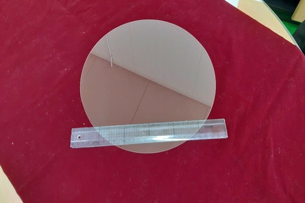
Daekyung Semco, which specialized in ceramic semiconductor and display materials, announced on Monday that it succeeded in developing 12-inch sapphire wafer with high quality recently.
Sapphire wafer is used to manufacture high-power semiconductor and thin film semiconductor as well as LED. Because there was not any company in South Korea that was able to manufacture 12-inch sapphire wafer, it is currently imported from Rubicon Technology based in the U.S. that is the world’s biggest sapphire ingot manufacturer.
“We had been working with a major sapphire ingot manufacturer for the past three years and successfully developed 12-inch sapphire wafer.” said a representative for Daekyung Semco. “This development is the result of a small and medium-sized company doing everything it can for development of South Korean industries.”
The company also succeeded in materializing micro thin-film wafer with 0.5mm TTV (Total Thickness Variation) that surpasses the current standard at 0.7mm. It is currently working on developing 12-inch wafer with 0.3mm TTV.
The company recently built a production facility that is able to manufacture 3,000 sheets every month at its plant in Seongju-gun. Its 12-inch sapphire wafers will be manufactured from this facility and supplied to domestic and foreign customers for LED and high-power integrated circuit (IC) and as a carrier wafer for production of thin-film IC.
It recently supplied a prototype of its 12-inch sapphire wafer to foreign customers in Taiwan and others. If it is able to a sign an actual supply contact, it will be seen as one of top successful cases of localizing materials, components, and equipment.
There are other small and medium-sized companies that are looking to localize key materials used for mini-LED display.
LB Lusem announced that it was selected as the company that will oversee a national project on “development of challenging bonding materials and mini-LED module” that is being supported by the Ministry of Trade, Industry and Energy.
Most of materials that connect substrates and chips of mini-LED display come from Japanese companies while LED chip comes from Taiwanese and Chinese companies. The project will receive a government contribution of $15.5 million (18.4 billion KRW) until 2024 and focus on development of domestic bonding materials and mini-LED display through LED chip.
Multi-purpose binder materials for mounting mini-LED are developed by small and medium-sized companies based on fundamental technologies developed by Electronics and Telecommunications Research Institute. Research institutes and manufacturers will participate in the development of mini-LED chip. Various equipment needed for package manufacturing will be supplied by small and medium-sized companies.
“We are going to preoccupy next-generation markets by developing mini-LED module based on active matrix through domestic materials, components, and equipment.” said Choi Shin who is the manager of LB Lusem’s laboratory. “We are going to build a value chain for mini-LED display.”
Staff Reporter Yun, Heeseok | pioneer@etnews.com