SK Hynix is spurring the introduction of the extreme ultraviolet (EUV) process that is seen as the next-generation semiconductor manufacturing process. The company has been managing an EUV task force (TF) within the company’s research group and it has been taking a swift approach in applying an EUV production line to its new DRAM plant. SK Group is also taking initiatives by investing in related materials in order to prepare for an upcoming EUV era.
According to the industry on Monday, SK Hynix has been managing an EUV TF under its Future Technology Research Institute since the beginning of last year.
The company integrates every data related to the EUV process into the TF and conducts researches. Systems and equipment used for the EUV process are used during “lithography” process that repeatedly prints the shape of a circuit on a wafer through an EUV light.
It is heard that the TF divided processes related to the EUV process such as etching process and EUV mask manufacturing technology in detail and is conducting research and development (R&D).
It is heard that Jung Tae-woo who is the vice-president of SK Hynix is the leader of the TF. Vice-President Jung is an expert in the etching field who had participated in the development project of SK Hynix’s first 10nm DRAM “Arius” and a R&D process for a next-generation NAND flash memory. SK Hynix likely chose Vice-President Jung as the leader of the TF after considering the fact that the EUV process heavily involves lithography and etching processes. Aside from Vice-President Jung, many experts in the EUV process are involved in the TF.
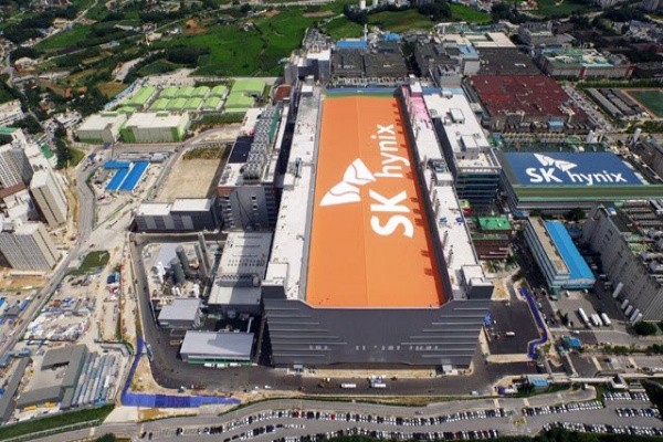
SK Hynix has also been putting in efforts to construct an EUV production line and it is planning to construct an EUV line at its new plant “M16” that is being constructed within its Icheon campus.
The company made a statement last year that it would apply the EUV process starting from its next-generation 1a (4th generation 10nm DRAM) chip in 2021.
SK Group is also preparing to welcome an EUV era by investing or acquiring promising EUV materials makers in South Korea and foreign countries.
Because the wavelength of an EUV light is one fourteenth of that of an ArF light that is being used for the current lithography process, the EUV process can be used to print fine patterns and is seen as the next-generation semiconductor manufacturing process. It is heard that Samsung Electronics and Taiwan-based TSMC are forming a rivalry by establishing EUV-related infrastructures early.
However, experts from the industry believe that SK Hynix also possesses stable EUV process technologies for DRAM that are just as advanced as that of its competitors.
“Although it is true that SK Hynix started working on related technologies later than its competitors, it is quickly securing related technologies through its systematic system and an active support from its parent company.” said a representative for the industry.
Staff Reporter Kang, Hyeryung | kang@etnews.com