SK Hynix will expand their non-memory semiconductor foundry business . Unlike how Samsung Electronics concentrates on the foundry business applying the 14 nano FinFET process, they focused on expanding the 8-inch(200㎜) 90 nanometer process, in order to prepare a small production system for various system semiconductors.
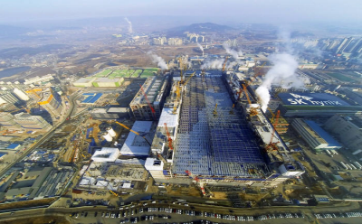
SK Hynix has been rearranging production lines to increase the types of chips produced at Cheongju M8 fab that provides system semiconductor foundry service.
At M8 fab, CMOS238 Image Sensor(CIS), Power Management IC(PMIC), and Display Driver IC(DDI)을 are mainly produced. Nand Flash had also been produced once, but since the third quarter of 2012, all were changed into exclusive fabs for non-memory semiconductors.
It seems SK Hynix will move non-memory semiconductors, such as CIS, produced in the 8-inch fab to the 12-inch(300㎜) fab, and the 8-inch fab will produce new non-memory semiconductors. Since the quantity of non-memory semiconductors originally produced at the 8-inch fab is large, the production more than doubles when switched to the 12-inch fab. This is economical, since the production cost is reduced that much. SK Hynix introduced a 12-inch non-memory semiconductor equipment for research last year, and ever since, have additionally purchased and been using another equipment for development.
Line M8 is planning to maintain its 8-inch, while modifying the non-memory semiconductors being produced and increasing the number of types. They are planning to operate in an adequate way for small quantity batch production, in preparation for an increase in demand for production of diverse types of non-memory chips, as an era of Internet of Things(IoT) awaits.
SK Hynix has started the expansion of their foundry business by recruiting massive manpower in the non-memory field, along with changing production lines, etc. Industry process experts and fabless industry researchers have newly moved in.
Staff Reporter Bae,okjin withok@etnews.com
The reason why SK Hynix is maintaining the 8-inch fab instead of investing in high-tech process seems to be so as to focus more on collecting small quantity batch production know-how than on massive investment. Samsung Electronics has applied the 14 nano FinFET technology to the non-memory field and TSMC of Taiwan is also in preparation for commercializing the 16 nano FinFET processing technology. Since SK Hynix is a late starter and needs massive investments and a long period of time to secure high-tech processing technology, they seem to be taking the strategy of expanding existing know-how to take actions against the age of IoT.
The business world has predicted that SK Hynix will put priority on securing many domestic fablesses using Taiwanese foundries as client companies. By examining items that are under development in domestic fablesses or are expected to increase in production, and stably securing client companies, they are building foundry know-how and technical skills.
A fabless official said, “There are many fablesses that inevitably use Taiwanese fabs because Samsung Electronics foundries require a certain scale of production and have advanced processing technology so that they cannot meet the conditions. If there is no need of high-tech processing and small quantities can be produced, it is good news for domestic fablesses since there is no need to use Taiwanese fabs.”
SK Hynix said, “We are examining the plan to move the equipment in M10 to M14, and utilizing the remaining space of M10 as a lab or for non-memory semiconductor production . Nothing has been confirmed about non-memory semiconductor production, introduction of mass production equipment, etc. at the 12-inch line.”
Staff Reporter Bae, Ok-jin | withok@etnews.com