Application of process on the 1 of semiconductor mass production lines
Proof of 'Localization' to escape relying on imports for the entire amount
Key is the expansion of exposure process utilization
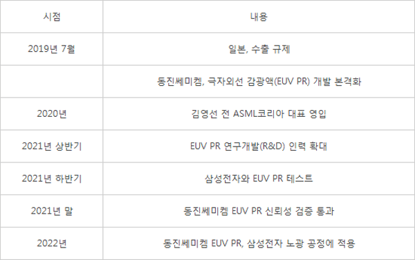
Samsung Electronics introduced extreme ultraviolet (EUV) photoresist(PR) for high-tech processes developed by a Korean company to their mass production line. This is the result after three years of flat-out efforts for localization due to Japan's export regulations in 2019.
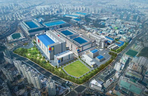
Samsung Electronics was found to be using Dongjin Semichem EUV PR for one of their semiconductor process (layer) lines. It was applied to the mass production line less than a year after Dongjin Semichem's EUV PR passed Samsung Electronics' reliability test (Qual) last year. One process line is only a very small part of Samsung Electronics' entire process. However, as it is a product that was entirely dependent on imports, it has a special meaning.
Dongjin Semichem jumped into product development when Samsung Electronics attempted to reorganize their EUV PR supply chain after Japan's export restrictions. In 2020, Young-sun Kim, former CEO of ASML Korea, was recruited as vice chairman to lay the groundwork for advancing into the EUV PR business. Early last year, they accelerated product development by securing additional EUV PR research and development (R&D) personnel.
Dongjin Semichem's EUV PR went through several months of verification at Samsung's Hwaseong Campus. It is known that Joon-hyeok Lee, vice chairman of Dongjin Semichem, directly took the lead until before the reliability test was conducted. Although it passed reliability verification at the end of last year, the actual application to mass production lines was unclear.
As Samsung used this product for actual semiconductor production, Dongjin Semichem became the first company to localize EUV PR to the level of mass production. YOUNGCHANG Chemical and SK materials performance are also developing EUV PR, but they have not yet reached the level of reliability verification.
It is still not decided if Samsung Electronics will introduce additional EUV PR from Dongjin Semichem. This is because there are many factors to consider, such as relationships with overseas EUV PR suppliers. It is also important that Dongjin Semichem EUV PR shows stable performance in other layers. EUV PR can be applied to 3 to 50 exposure processes such as metal·implant·via. It has not been confirmed which process Dongjin Semichem products are used for. As the supply volume is small, it is expected that the performance of Dongjin Semichem's will decide whether additional supply will be expanded in the future. Samsung Electronics and Dongjin Semichem saved their breath by saying, “We cannot officially confirm any details regarding the supply.”
◇Explanation of Terminology
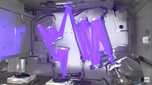
EUV PR = It is called photoresist and is a key material in the semiconductor exposure process. When applied on a wafer and exposed to light with semiconductor exposure equipment, it changes its physical properties from a chemical reaction. If the PR is washed off leaving only the necessary parts with a developer, a microcircuit is drawn. EUV exposure equipment is required to draw ultra-fine circuits, and the PR used in this process. Previously, the market was 100% dependent on imports from Japan and other countries.
[The log of Dongjin Semichem EUV PR localization]
By Staff Reporters Dong-jun Kwon (djkwon@etnews.com)
Ji-woong Kim (jw0316@etnews.com)