Zeiss Korea is building a R&D center for semiconductors and electron microscopes in Korea. They will pour in funds reaching 50 billion KRW over 4 years. They will cooperate with semiconductor manufacturers and clients to develop new equipment. With plans to open as early as next year, they began recruiting a workforce.
Zeiss Korea revealed the state of Zeiss’ optical and optoelectronic solution business and their future plans at the ‘Zeiss Korea Innovation Center’ in Dongtan, Gyeonggido on the 23rd. Hyeonseok Jeong, the CEO of Zeiss Korea, said that, “We are planning to build electron microscope R&D facilities and semiconductor R&D facilities. ”He went on to say, “Investments will begin in earnest starting next year, and we have investment plans for 48 billion KRW over 4 years.” The 20 million USD of investments the Ministry of Trade, Industry, and Energy successfully attracted for ASML, ASM, and Zeiss includes a portion for Zeiss.
This is the first time that Zeiss is building an electron microscope R&D facility outside of Germany. The semiconductor R&D facility is the first in Asia as well.Their goal is to begin the operation of their R&D facilities by next year. They are currently seeking to secure a workforce.
Zeiss Korea is planning to develop equipment tailored for Korea to respond to the demands of electron microscopes and semiconductor equipment, which are their main solutions. The electron microscope R&D facility will respond to the demands for measurement needed to manage quality and improve performance in a wide range of industries, such as semiconductors, batteries, aviation, space, and automobiles. It appears that it was judged that Korea had sufficient marketability due to the many industries that require electron microscopes.CEO Jeong said that, “Korea’s companies are at the forefront of automation solutions,” and went on to say that, “We are investing in the field of electron microscopes so that we can develop products closer to our clients.”
The construction of the semiconductor R&D facility is also to develop products that are also tailored to the demands of clients. As the proportion of the semiconductor business in Zeiss Korea rose recently, the demand for independent product development is rising as well. They plan to make new solutions with semiconductor manufacturers and their clients at the semiconductor R&D facility. They are looking into candidates like wafer quality measurement equipment.
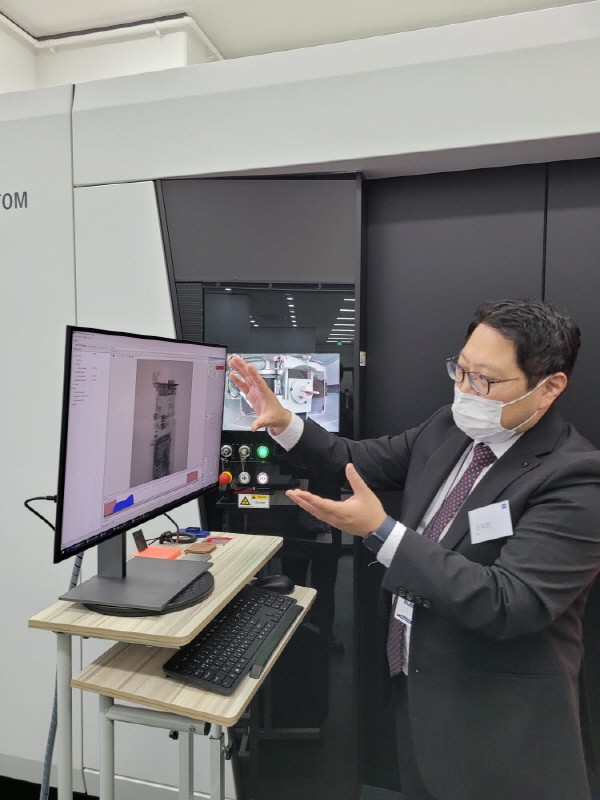
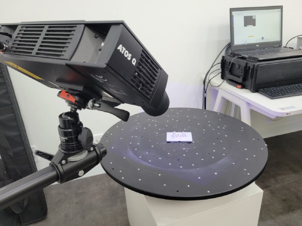
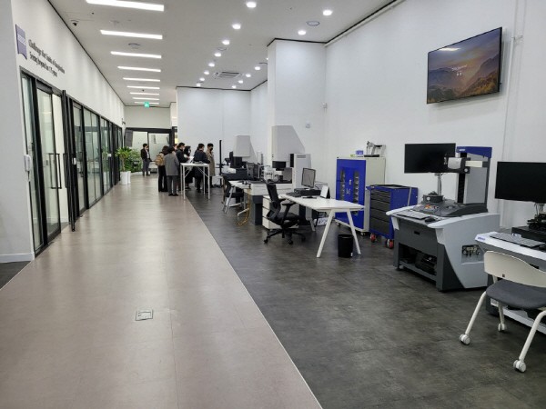
They also revealed the Zeiss Korea Innovation Center on the same day. They showcased various optical and X-ray equipment needed in the development of things like semiconductors, cars, and batteries, as well as 3D measurement machines and high-resolution computed tomography (CT) equipment. The center was opened last August so that clients can directly experience Zeiss’ solutions and jointly discover new applications. It is also in charge of Zeiss’ solution training and service. Since its opening, it has drawn enough attention to accumulate over 100 visits from clients.
◇Zeiss = A global optical and optoelectronic engineering company established in 1846, it is headquartered in Germany. They are the sole suppliers of lenses and optical equipment to ASML. 80% of the entire world’s semiconductors use Zeiss’ technology for production. Zeiss Korea was established in 1986 and runs 6 offices. They have over 330 employees and Zeiss’ sales reach 4th place, with their presence in over 50 coutnries.
Reporter Dongjoon Kwon djkwon@etnews.com