Intel is adopting 'High NA', a next-generation extreme ultra-violet (EUV) exposure equipment, to a U.S. semiconductor plant. High NA is EUV exposure equipment developed by ASML, and it is the first time to be adopted into a semiconductor manufacturing process. It is noteworthy whether it will be applied advantageously to Intel, which is competing with TSMC and Samsung Electronics for the commercialization of ultra-fine semiconductor chips.
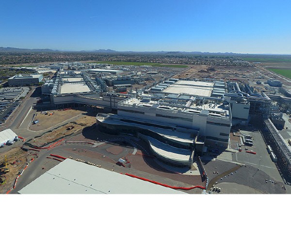
Intel announced on the 19th that they are adopting the next-generation EUV exposure equipment 'High NA' to their Oregon plant in the U.S. Intel explained, "We will maintain our leading position in semiconductors by introducing ASML high NA equipment, the world's largest equipment maker." Ann Kelleher, executive vice president of Intel said, "We will continue to pursue 'Moore's Law' with close cooperation with ASML." It is interpreted as meaning to achieve the development of semiconductor technology.

Intel is the first in the industry to adopt high NA and produce chips in 2024 with the '20A' (Angstrom) process. High NA is the new EUV exposure equipment developed by ASML. After announcing re-entry into the foundry market that produces semiconductor chips in March of last year, Intel announced that they would complete the 20A process technology, which is at the level of the 2㎚ process. Intel's chip production is scheduled for 2024. Intel has recently secured Qualcomm, a leading mobile AP, as a foundry customer, and is expected to produce cutting-edge chips using the foundry ultra-fine process.
The introduction of Intel and ASML High NA is interpreted as Pat Gelsinger's bold move in the foundry market.
ASML is the exclusive supplier of EUV exposure equipment required for advanced micro processing. High NA EUV equipment can draw microcircuits less often than before. It is characterized by raising the lens’ numerical aperture (NA) from 0.33 to 0.55. This reduces the number of masks engraved with circuit patterns, thereby reducing costs and shortening process times.
Intel plans to target the foundry market by preemptively securing high NA equipment. In the foundry market where TSMC and Samsung Electronics compete, Intel must promote the growth of the foundry market by introducing a 4nm or less process. With the introduction of fine processes in the foundry process, it is expected that the number of chips such as high value-added APs will increase. It is necessary to introduce a 3nm advanced microprocessor that Samsung and TSMC are challenging for mass production. After Intel enters the foundry market, ASML cooperation is expected to have a significant impact on the foundry market as a new high-tech semiconductor company appears.
By Staff Reporter Ji-woong Kim (jw0316@etnews.com)