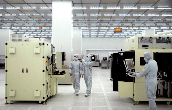
Nepes Laweh, a semiconductor packaging subsidiary of Nepes, will double the production capacity of ‘Fan-out-Panel Level Packaging (FO-PLP)', a next-generation packaging process. It is a strategy to respond to the increase in demand from global semiconductor customers and to raise mass production capacity.
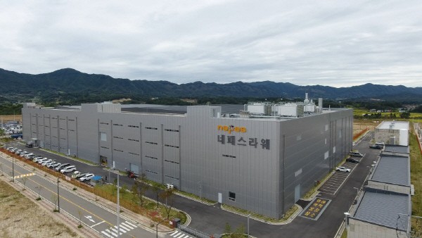
Nepes Laweh held a ceremony for the completion of the FO-PLP line at the Cheongan Campus on the 7th, and Minister of Trade, Industry and Energy Seung-wook Moon, Chungbuk Province Governor Si-jong Lee, and representatives of customers and partners attended the event. The company completed the power management integrated circuits (PMIC) certification from the global semiconductor company in the third quarter, and started mass production. Nepes Laweh is the first to mass-produce PMIC using FO-PLP.
Nepes Laweh will double its FO-PLP production capacity next year. It will expand the production infrastructure according to the increase in customer's PMIC demand. Previously, Nepes announced that it would invest KRW 120 billion to expand the FO-PLP by next September.
The fab that held the completion ceremony was the first fab built on the 186,000 m² (56,000 pyeong) Cheongan campus site, equivalent to 25 soccer fields. Based on the dimension of 600mm FO-PLP, the fab can produce up to 96,000 sheets per year. The president of Nepes Semiconductor, Chil-hee Chung, said, “Nepes Laweh, which has presented the world standard for FO-PLP production systems, will play a role as a stepping stone in establishing a new back-end process ecosystem in Korea.”
Nepes provides advanced system semiconductor high-density packaging solutions for each application such as smartphones, automobiles, and Internet of Things (IoT) as a next generation packing. Chairman Chung said, “FO-PLP is an optimal packaging solution for high-end semiconductors resulting from a long cooperation with domestic and foreign partners such as materials, parts, and equipment. Nepes will continue to work closely with its partners to provide advanced technology packaging solutions.”
Minister Moon congratulated on the completion of the new plant in Nepes Laweh, and emphasized the importance of advanced packaging technology. He said, “This year, we will promote a large-scale preliminary feasibility project for an advanced packaging platform to support the performance of the packaging industry. We plan to increase the budget for the packaging specialist training project by 50% next year.” The Ministry of Trade, Industry and Energy will gather suggetions from industry, academia, and research institutes to prepare comprehensive measures to expand the base of the packaging industry in the first half of next year.
<Glossary>
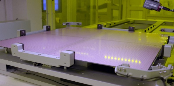
◇Fan-out-Panel Level Package (FO-PLP) = One of the next-generation packaging technologies. Fan-out (FO) technology that can increase the number of input/output terminals (I/O) by placing semiconductor I/Os outside the chip, and panel-level packaging (PLP) that directly connects and combines packages chips and devices on a rectangular panel. The rectangular shape makes it possible to minimize the discarded edges and produce more chips compared to the round shape. Nepes' 600mm square panel can make five times as many chips (Die) as one 12-inch wafer.
By Staff Reporter Dong-jun Kwon (djkwon@etnews.com)