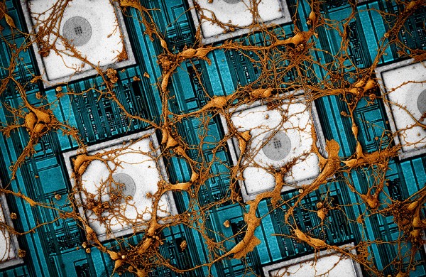
Researchers at Samsung Electronics and Harvard University in the United States presented a vision for the next-generation neuromorphic semiconductor chip through 'copying' and 'pasting' the brain neural network as it is. The neuromorphic semiconductors mimic the neural networks of animals and humans, aiming to reproduce high-level functions of the brain such as cognition and reasoning.
Samsung Electronics announced on the 26ththat 'Neuromorphic Electronics based on Copying and Pasting the Brain' was published on 23rd (UK time) in the world-renowned scientific journal Nature Electronics. This paper was written by Don-hee Ham, a fellow at Samsung Electronics Advanced Institute of Technology and a professor at Harvard University in the US, Professor Hong-geun Park at Harvard University, President Seong-woo Hwang of Samsung SDS, and Vice President Ki-nam Kim of Samsung Electronics. It is attracting attention for combining neuroscience and memory technology and presenting a vision for next-generation AI semiconductors, with the participation of technology leaders from academia and industry.
This paper contains the vision of a neuromorphic chip technology that reproduces the brain's unique functions by measuring the electrical signals of neurons in the brain neural network, copying the connection map between neurons, and pasting the copied map into a memory semiconductor.
First, a neural network map is copied through ultra-sensitive measurement that directly penetrates nano-electrodes into neurons. It was difficult to penetrate electrodes into neurons in the past, with the recent advancement of nanotechnology. But now, it is possible to arrange nano-electrodes inside microscopic neurons and read simultaneously insignificant electrical signals generated at the contact points (synapses) between neurons. This then maps the brain neural network by finding the contact points between neurons. Samsung Electronics and Harvard University have been researching on this technology in collaboration since 2019. The aim of this paper is to present a completely new concept of neuromorphic semiconductor, in which each memory acts as a contact point between neurons by pasting the copied neural network map into a memory semiconductor.
The paper also proposed a groundbreaking technology perspective that directly drives the memory platform with the measurement signal obtained through radiation. This can significantly reduce the time to construct a neural network map compared to analyzing a large amount of signals measured in a neural network with a computer. This platform can be used for commonly used memory, such as flash, and other types of nonvolatile memory, such as resistive memory (RRAM).
To realize about 100 trillion neurons in the human brain as a memory network, the memory density must be maximized. To this end, Samsung Electronics proposed using cutting-edge semiconductor technologies such as 3D flash stacking technology and TSV (Through Silicon Via) 3D packaging, which are applied to high-performance DRAM.
Don-hee Ham, a fellow at Samsung Electronics Advanced Institute of Technology, said, “The bold approach proposed in this paper will help to broaden the boundaries of memory and system semiconductor technologies and further develop neuromorphic technologies.”
By Kwon Dong-jun, staff reporter djkwon@etnews.com