NextIn Solutions collaborated with Intel and it has developed a 3D inspection system. It is the first semiconductor wafer inspection system developed by the industry and it is expected to be very helpful in rapidly inspecting multi-layer semiconductors. Some also predict that NextIn will be the first South Korean semiconductor equipment manufacturer to supply semiconductor equipment to Intel.
NextIn recently introduced an advanced inspection system called “NIR (Near Infrared Ray) TSOM (Through-focus Scanning Optical Microscopy) 3D memory inspection system” at “SPIE Conferences”.
This system was developed in order to inspect 3D memory wafers such as NAND flash that vertically stack information storage spaces.
As multi-layer NAND flashes with more than 170 layers have started to make their appearances, it has become difficult to find various particles that are located at the very bottom of the layer and faulty circuits. This can lead to poorer wafer productivity and yield.
NextIn and Intel have found a solution through NIR and TSOM technique. Method of inspecting a wafer that is finished with etching process is similar to principle of photography. Currently, defects are detected by focusing (in-focus) on each area that needs to be inspected and taking pictures of the areas.
However, NIR TSOM technique intentionally takes many pictures with out of focus and gathers the pictures to one place in order to separate acceptable products from defects. While one picture may look obscure, gathering many pictures and selecting a common defect can lead to much faster and accurate inspection. The technique does not require a separate comparison model as well.
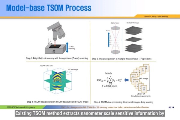
The technique uses NIR as the light source. NIR has a longer wavelength than UV that is currently used for inspection systems. Although NIR produces less clear images due to its resolution being relatively low, its long wavelength enables it to penetrate deep inside the memory and conduct inspection. NextIn’s NIR TSOM technique’s performance is also upgraded so that it is able to penetrate much deeper inside the memory than the first NIR TSOM technique that was developed in 2016.
“If devices are like a single-family house, 3D devices that have been developed recently are like super-tall apartments.” said President Park Tae-hoon of NextIn. “NIR TSOM technique is like finding a trash in a flower garden that is located on the ground between many tall apartments in the air.”
NextIn has traditionally been an inspection system manufacturer and it has been competing against KLA based in the United States and Hitachi from Japan in the dark-field inspection system field.
However, it is looking to enter the bright-field inspection system field by developing NIR TSOM inspection system with an upgrade performance. Compared to dark-field inspection systems, bright-field inspection systems are much more difficult to develop and are more expensive as well. KLA and Applied Materials own overwhelming market shares in the field currently.
What make this development more special is that it involved collaboration with Intel. By successfully developing an advanced inspection system with the world’s biggest chip maker, NextIn may be the first South Korean semiconductor equipment maker to supply its equipment to Intel.
One official from the industry predicted that Intel may utilize NextIn’s inspection system for Optane memory production lines.
Staff Reporter Kang, Hyeryung | kang@etnews.com