WONIK IPS, which is the second biggest semiconductor equipment manufacturer in South Korea, has localized “metal CVD (Chemical Vapor Deposition)” system that is a key system for the front-end-of-line (FEOL) processing and currently comes from TEL based in Japan. The semiconductor industry in South Korea has its eyes fixed on the development as there is a great chance that WONIK IPS’ metal CVD system will continue to develop hereafter.
According to the industry on Wednesday, WONIK IPS supplied its NOA system for the first time to SK Hynix’s M15 fab in Cheongju. The M15 fab is one of SK Hynix’s key NAND flash plants that manufactures 128-layer NAND flash memories and others.
Metal CVD system is used during metal wiring process that is one of eight important processes of semiconductor manufacturing. The process is part of the FEOL processing that connects metallic wire to integrated circuit so that there is a good flow of electric signals.
Metallic wire is usually made out of copper, tungsten, or aluminum that has low electric resistance and excellent adhesiveness. The issue is that particles of metallic wire tend to penetrate “insulator film” that plays an important role within a semiconductor device. Without a proper measure, metallic wire can greatly reduce the quality of a product by negatively affecting the performance of insulator film.
To prevent this penetration issue, a thin preventive film is placed between metallic wire and insulator film to prevent the mixing of the two. This film is called metallic barrier and it is usually made out of titanium or titanium nitride.
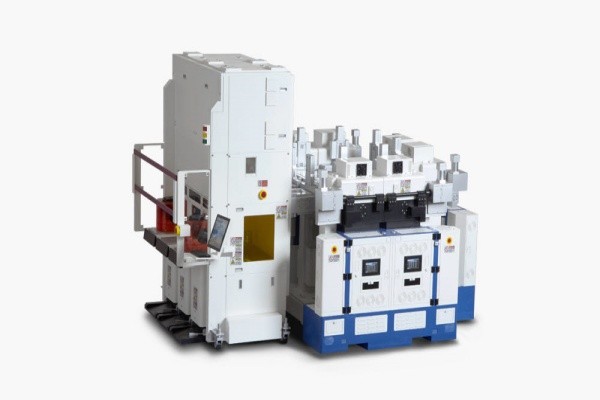
It is understood that WONIK IPS’ metal CVD system is used to create metallic barriers. NOA system can also be used for tungsten metal wiring process and atomic layer deposition technique that is seen as a next-generation deposition technique. As a result, possible applications of the company’s metal CVD system will be infinite.
Localization of metal CVD system by WONIK IPS is very meaningful from the fact that no other South Korean companies have been able to commercialize their own metal CVD systems.
Until now, the market is led by TEL that possesses outstanding technologies in this field. It is reported that TEL owns a significant portion of the market share as SK Hynix included metal CVD system to a list of products that might need domestic replacements when the Japan-South Korea trade dispute started to become a huge issue.
After three long years of R&D, WONIK IPS was able to supply its own metal CVD system to one of SK Hynix’s state-of-the-art facilities. Although the company has a different metal CVD system aside from NOA, the other system does not have appropriate capabilities to be used for major processes of the top semiconductor manufacturers in South Korea.
The industry sees the performance of NOA system almost equivalent to that of TEL’s metal CVD system when it comes to step coverage, yield, wafer productivity and others. Also, it is understood that there are various tests taking place in order for NOA system to be used by Samsung Electronics for its production lines in Hwaseong and Pyeongtaek.
One representative from the semiconductor equipment industry gave an evaluation on NOA by saying that it is incredible for WONIK IPS to develop its own metal CVD system even without having to use technologies patented by other global companies.
Meanwhile, WONIK IPS has successfully localized various deposition systems that are used for NAND flash memories.
It recently localized molding process system that deposits oxide and nitride substances alternatively and delivered it to Samsung Electronics’ Xian NAND manufacturing fab. This system is also used for NAND flash memories with more than 100 layers.
Staff Reporter Kang, Hyeryung | kang@etnews.com