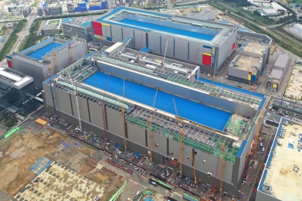
Samsung Electronics has begun operating its “Pyeongtaek Line 2 (P2)” that is the world’s biggest semiconductor plant. The P2 fab is one of Samsung Electronics’ key semiconductor production bases and it spans more than 128,900 m2 that is equivalent to 16 soccer fields.
Samsung Electronics is going to invest $25.4 billion (30 trillion KRW) in the P2 fab and secure a line that will manufacture DRAM, NAND flash memory, and system semiconductor in order to achieve “super gap within the global semiconductor industry”.
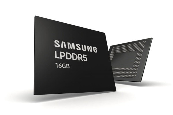
Samsung Electronics announced on August 30 that it has started shipping DRAMs by operating the P2 fab. The company explained that it is currently mass-producing the industry’s first 16Gb LPDDR5 mobile DRAM using extreme ultraviolet (EUV) technology built on its 3rd generation 10nm-class (1z) process.
EUV technology is the latest photolithography technology used to materialize integrated circuit (IC) and it is the only technology that is able to materialize IC pattern under 7nm.
The new DRAM that the company is mass-producing will be used for flagship smartphones and it has operational speed of 6,400 Mb/s that is about 16% faster than that of the 12Gb LPDDR5 (5,500Mb/s) that is widely used in today’s flagship smartphones. It is able to process 51.2GB in just one second that is equivalent to about 10 5Gb full HD movies when made into a 16GB package.
Back in March, Samsung Electronics stated that it delivered DRAMs, which were built on its 1st generation 10nm-class (1x) process using EUV technology, to customers. However, it only supplied one million DDR4 DRAM modules at that time.
According to the industry, it is heard that the DRAM production line at the P2 fab is able to manufacture 35,000 to 40,000 12-inch wafers per month. The line is only constructed partially at the moment. A semiconductor facility will typically have its structure built first and be equipped with necessary equipment depending on a product.
DRAM shipments from the P2 fab indicates that the fab, which is an important strategic base for Samsung Electronics’ semiconductor business, has entered a full-scale operating system. Samsung Electronics is also constructing a foundry production line and a NAND flash memory production line at the P2 fab. It broke ground for the new foundry production line back in May while the ground was broken for the NAND flash memory production line in June. The company is working on cleanrooms and it expects to operate the two lines in the second half net year.
It is expected that the P2 fab will further solidify Samsung Electronics’ position as the world’s top DRAM and NAND flash memory manufacturer. One’s competitive edge is determined by the number of latest products it manufactures. The fab is also expected to be a huge help for Samsung Foundry. Although Samsung Electronics is currently ranked second within the global foundry market, its foundry business is growing at a rapid rate as it recently achieved its best quarterly performance in the past second quarter.
Potential economic impact by the P2 fab is also drawing interests from many people. Once it is fully equipped, it will have a production capacity of about 200,000 wafers. Its production capacity and its size are the biggest in the world. The construction of the P2 fab is expected to create about 30,000 jobs as Samsung Electronics will hire about 4,000 people by itself while its partnering companies and construction companies are expected to hire about 26,000 people.
Despite many global uncertainties such as the COVID-19 pandemic, Samsung Electronics continues to speed up its investments in its semiconductor business. Vice Chairman Lee Jae-yong of Samsung Electronics once announced that the company needs to secure competitive edge in fundamental technologies through continuous investments in the midst of crisis and is emphasizing the importance of securing leadership in fundamental technologies.
Samsung Electronics plans to preoccupy future markets through active investments. “The 1z-based 16Gb LPDDR5 is a product that has overcome the most difficult development process and it was developed to break through limitations in microfabrication.” said Lee Jung-bae who is the vice president of Samsung Electronics’ Memory Business Division’s DRAM Development section. “By continuing to develop premium DRAMs, we will be able to quickly respond to demands for latest memories.”
Staff Reporter Kang, Hyeryung | kang@etnews.com