S&S Tech Corporation, a South Korea-based semiconductor materials maker, is spurring development and production of key materials for the EUV (Extreme Ultraviolet) process. It is heard that the company has secured advanced technologies in the field of EUV pellicle that has yet to be commercialized anywhere in the world.
According to the industry on June 18, S&S Tech recently made a public announcement that it decided to invest $8.25 million (10 billion KRW) in development and production of blank mask and pellicle that are key materials for the EUV process. This amount is equivalent to about 11% of S&S Tech’s capital ($73 million (88.5 billion KRW)) and annual sales ($69.6 million (84.4 billion KRW)).
S&S Tech engages in the manufacture of blank masks that are used during the photolithography process. During a photolithography process that repeatedly imprints the patterns of integrated circuits on silicon wafers, “mask” is used to help the light hold the pattern of an integrated circuit. Blank mask indicates a mask before it is imprinted with the pattern of an integrated circuit.
S&S Tech has been supplying blank masks that are used for the ArF lithography process that is currently the most common photolithography process within the industry.
It has now shifted its attention towards pellicle and blank mask for the EUV lithography process in order to deal with the coming of the EUV era as semiconductors become smaller and smaller.
If S&S Tech succeeds in manufacturing especially pellicles used for the EUV lithography process, it will draw many eyes from the global semiconductor industry as no company in the world has yet to commercialize such pellicle.
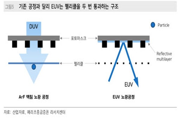
Pellicle is like a “protective cover” for a mask and it can improve the effectiveness of a process by raising utilization of masks that are expensive to manufacture and lowering contamination level.
It is extremely difficult to develop EUV pellicle technology. The EUV lithography process is based on “reflection” rather than “penetration” that is the basis of the ArF lithography process. Because EUV light is absorbed into every material, EUV masks are made up of materials that reflect EUV light.
In order for an EUV pellicle to properly protect an EUV mask, it needs to have properties that absorb and reflect an EUV light. As a result, the degree of EUV pellicle technology is very high.
However, because the technology has to be developed one day in order to increase production efficiency, many domestic and foreign companies are working hard to be the first one to commercialize it.
It is heard that many foreign companies such as TSMC based in Taiwan, Mitsui Chemicals based in Japan, and Teledyne based in Canada are committing many hours to develop EUV pellicle.
Out of all companies, S&S Tech is the one that has shown the most process in development. While it is said that EUV pellicle with EUV light penetration rate of 90% can be used in actual production, S&S Tech’s EUV pellicle recorded a rate of 88%.
“Although S&S Tech still needs to go through few steps before it is able to apply its EUV pellicle to actual production, it will be able to get there much faster with active support from buyers.” said a representative for the industry.
Through the official announcement, S&S Tech indicates that the end date for the investment will be June 30 of 2021. It is expected that it will be able to supply its EUV pellicle for actual production in the second half of 2021.
Meanwhile, S&S Tech has also been very active in researching EUV blank mask through transfer of technology.
The field is seen as a promising field as current powerhouses such as Hoya and Asahi Glass as well as Applied Materials, which is the world’s top company within the global semiconductor equipment industry, are also working on developing EUV blank mask.
Staff Reporter Kang, Hyeryung | kang@etnews.com