Samsung Electronics has begun supporting South Korea’s small and medium-sized semiconductor design companies (fabless). It developed a cloud-based design platform so that fabless companies can design semiconductor chips anywhere without having to establish a server and are providing lectures on cutting-edge processes.
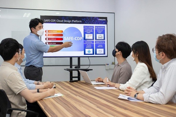
Samsung Electronics announced on June 18 that it launched “SAFE Cloud Design Platform (SAFE-CDP)” that allows its foundry customers to design semiconductor chips more easily.
The concept of this platform, which was developed by working with a platform company called Rescale, is that Samsung Electronics’ customers can design semiconductor chips at any time and anywhere as long as they have ideas through the platform.
The platform provides tools from EDA (Electronic Design Automation) software companies such as Ansys, Mentor, Cadence, and Synopsys within a public cloud.
Fabless companies have been feeling financial burdens from maintaining and managing their chip design programs as semiconductor chip design becomes more complicated and semiconductor chips become smaller. They have been investing in facilities and equipment such as tools that cost millions of dollars and increased servers within an office space.
However, Samsung Electronics’ SAFE-CDP reduces financial burdens for customers and allows them to use computing resources that are needed for chip design and verification with more flexibility.
SAFE-CDP will be especially useful for many small and medium-sized fabless companies in South Korea. For example, a semiconductor design house company called GAON CHIPS designed automotive semiconductor chip utilizing SAFE-CDP and found that it was able to reduce a necessary design period by 30% compared to before it utilized SAFE-CDP.
“Samsung Electronics’ SAFE-CDP will help lower entry barrier to the market for small and medium-sized fabless companies.” said CEO Jung Kyu-dong of GAON CHIPS that is also a design solution partner of Samsung Electronics.
In addition to GAON CHIPS, many small and medium-sized companies such as ADT and HANATEC announced their intentions to use the platform.
Samsung Electronics is actively pursuing cooperation with small and medium-sized fabless and design house companies after announcing its plan to strengthen South Korea’s system semiconductor ecosystem in April last year.
It decided to increase the number of times it offers its MPW (Multi Project Wafer) program, which is essential to develop prototypes of small and medium-sized fabless companies, to 3 to 4 times annually per process and offer 8-inch and 12-inch foundry services.
Also, it has been providing education on layout and design methodology and verification to fabless and design house companies since the second half of last year in order to raise their competitive edge.
“Our SAFE-CDP will be an important foundation helping fabless companies transition to a cloud-based design environment.” said Park Jae-hong who is the vice-president of Samsung Electronics DS division. “We are going to continue to make contributions so that our customers can launch innovative products by strengthening the foundry ecosystem in South Korea.”
Staff Reporter Kang, Hyeryung | kang@etnews.com