Semiconductor process that can create 3nm “single-patterning” through existing EUV (Extreme Ultraviolet) lithography system has been developed. Single-patterning indicates a process that patterns an integrated circuit on a wafer using a single exposure through a lithography system. Its production cost is greatly lower than that of “multi-patterning” that repeatedly patterns circuits.
The global semiconductor industry initially believed that 3nm EUV single-patterning process was only available through a next-generation “high-NA” lithography system. However, ASML and IMEC were able to carry out such process through existing lithography system. It is expected that semiconductor manufacturers such as Samsung Electronics will be able to reduce their investments in semiconductor equipment.
IMEC, a semiconductor research hub in Belgium, announced that it has implemented 3nm single-patterning technology through ASML’s 1st generation EUV lithography system “NXE:3400B”. IMEC also introduced its technology during a lithography conference of “SPIE” that is an international society for optics that was held in San Jose at the end of last year.
Lithography process is a key process for microfabrication and it repeatedly patterns integrated circuits on top of a wafer using light. While current lithography process mostly uses ArF light, semiconductor companies are rapidly adopting EUV light that is about one-fourteenth shorter than ArF light due to semiconductor microfabrication.
ASML, a semiconductor equipment maker from Netherland, is the only one that currently supplies EUV lithography systems. Samsung Electronics also uses ASML’s NXE:3400B.
The number of patterning is important during a lithography process. Although there is single-patterning technology, there are also multiple and quadruple-patterning technologies. Just like an intersection of a Venn diagram, thin parts that overlap due to repeated patterning is used as a circuit.
However, multi-patterning technologies cost more than single-patterning technology as they have to go through various preparations such as photoresist coating. This is the reason why semiconductor manufacturers prefer single-patterning over multi-patterning.
It is heard within the global semiconductor industry that ASML’s 1st generation EUV lithography system can implement single-patterning technology only at 7nm and 5nm processes. It was expected that 3nm single-patterning technology will be implemented through a next-generation High-NA system that features a 0.55NA lens.
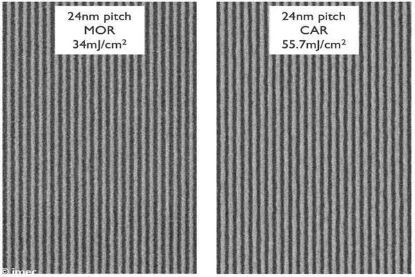
However, ASML and IMEC were able to pattern 24nm pitch lines using 3nm process and the current EUV lithography system by adjusting an incident angle of EUV light source.
“Due to the high incident angle of EUV light source, circuit’s image becomes distorted as light source goes through a photomask.” said IMEC. “We optimized an angle and found a way to minimize distortion of an image.”
Commercialization of such technology will be a positive news for South Korea’s semiconductor industry that is looking to adopt the EUV process as quickly as possible. As it will be able to introduce 3nm technology with a previously purchased 1st generation EUV system, it will be able to save its budget on equipment and increase durability of its current systems. While current EUV lithography systems are worth more than $126 million (150 billion KRW), next-generation High-NA EUV systems are expected to be worth more than $420 million (500 billion KRW).
“There is a chance that Micron Technology that has been hesitant in investing in an EUV system due to its expensive cost will be active in adopting the EUV lithography process.” said a representative for the industry. “This is an opportunity for the EUV market to grow.”
Meanwhile, ASML is dealing with the current trend of the EUV process by accelerating the development of a next-generation High-NA lithography system called “EXE:5000”.
Staff Reporter Kang, Hyeryung | kang@etnews.com