WONIK IPS is drawing eyes from the industry as it is planning to supply “domestic molding system” to Samsung Electronics. This system is absolutely needed for 3D NAND device fabrication and it has been imported from foreign companies for a while.
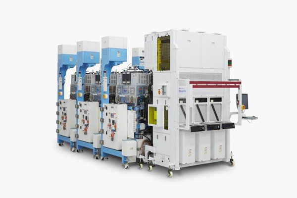
According to the industry, it is understood that WONIK IPS obtained an order for new molding systems (Quanta Gen 5 and 6) from Samsung Electronics.
These systems will be installed within Samsung Electronics’ second 3D NAND fab in Xi’an and they will be used to manufacture high-end 3D NAND flash memories.
Although the exact number of systems that WONIK IPS will deliver to Samsung Electronics has yet to be confirmed, the industry believes that the order will significantly boost WONIK IPS’ performance.
3D NAND flash memory is a semiconductor that has better storage capacity as the memory cells are stacked vertically. Thin films that are made up of “oxide” and “nitride” need to be stacked layer upon layer. This process is called molding process. Molding system helps oxide and nitride films to be stacked evenly. Performance of a molding system is critical when the number of layers goes over 100.
This is not the first time WONIK IPS supplied its molding system to Samsung Electronics as it supplied molding systems in 2014 for Samsung Electronics’ first 3D NAND fab in Xi’an.
However, there has barely been any transaction between WONIK IPS and Samsung Electronics after 2017 as a multinational semiconductor equipment maker called Lam Research has been showing strength. It is heard that Lam Research had obtained entire orders from Samsung Electronics for a while. In order to take back orders from Lam Research, WONIK IPS has strengthened its R&D and drastically upgraded the performance of its systems and succeeded in obtaining an order from Samsung Electronics.
WONIK IPS has increased the productivity of its Quanta system by increasing plasma density and the number of chambers. The biggest feature of its Quanta system is its ability to create even oxide and nitride films and deal with production of NAND flash memories with number of layers of over 100.
“Although Lam Research has also obtained an order for molding system from Samsung Electronics, it is meaningful that WONIK IPS’ molding system has reentered Samsung Electronics’ key semiconductor process.” said a representative for the industry. “It is understood that WONIK IPS’ new molding system is better than Lam Research’s molding system when it comes to evenness of thin films.”
It is heard that WONIK IPS has also won orders for system semiconductor deposition system that will be used for EUV line in Hwaseong and semiconductor systems that will be used for the second 10nm DRAM fab in Pyeongtaek. It is estimated these orders are worth $580 million (700 billion KRW). It is heard that WONIK IPS is looking into expanding its plant in order to deal with increased orders.
“There is a chance that WONIK IPS will be able to make its greatest annual sales in 2020.” said a representative for the semiconductor equipment industry
Staff Reporter Kang, Hyeryung | kang@etnews.com