Small to midsize South Korean company has succeeded in manufacturing copper plating solution for semiconductors, which is currently imported from Japan and the U.S. It will be interesting to see whether this localization will start a trend of localization within the field of copper plating solution that is one of key materials for back-end process of microfabrication of semiconductors.
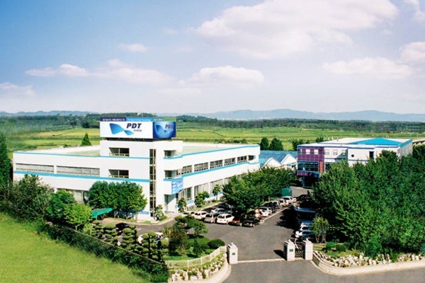
PDT (CEO Song Hak-bong), which manufactures equipment and systems for semiconductor, display, and automation, announced that it has become the first South Korean company to produce copper plating solution that is used for TSV (Through Silicon Via) process and semiconductor bumping process.
PDT either finished going through evaluations of the quality of its copper plating solution by major semiconductor companies or is currently going through them. It also added that it has developed plating solution for redistribution layer.
Plating solution is used for 3D TSV process and bumping process that are used to increase the level of integration of chips. In case of bumping process, solder bump is formed by forming plating layers using copper plating solution and Sn-Ag plating solution and removing photoresist through etching process.
Copper plating solution is also used for TSV process that is used to stack chips. Copper seed layers are formed through formation of gaps through photolithography and etching processes and deposition. Afterwards, chips are connected with each other after going through TSV gap fill process that fills gaps with copper plating solution.

Key to copper plating solution is organic additives that control the shape of plating. PDT emphasized that its copper plating solution can control the shape of plating by controlling the composition of organic additives so that plating process can be performed fast and with reliability. Shape of plating whether it is concaved up, flat, or concaved down can be adjusted according to needs.
PDT predicts that the copper plating market will grow quickly as demands for state-of-the-art packing are increasing due to rapid increase in demands for high integrated semiconductors. Market research company called Yole Developpement estimated that the copper plating solution market and the Sn-Ag plating solution market were worth $300 million in 2018.
“Japanese and American companies control our copper plating solution and Sn-Ag plating solution markets and Japanese companies control our Sn-Ag plating solution market especially.” said a representative for PDT. “We have currently prepared a portfolio for copper plating solution for back-end process and we are currently developing Sn-Ag plating solution and we are planning to apply for relevant patents towards the end of this year.”
PDT, which was established in 1992, has been supplying CNC machines for mobile devices, PCB-related automation system, and LCD module system. It has recently started working on electronic material business and it currently has its own brands such as copper plating solution called ‘Smartplate’, Sn-Ag plating solution called ‘SmartCap’, and ‘SmartVia’ that reduces the speed of plating more than its competitors.
Staff Reporter Bae, Okjin | withok@etnews.com