EUV (Extreme Ultraviolet) lithography process is drawing attention as the next major semiconductor technology. Samsung Electronics’ APs (Application Processor) based on 7nm EUV process are being produced and it is expected that 5nm and 3nm EUV processes will be implemented in couple years. Samsung Electronics is planning to operate its production line for EUV lithography sometime during the first half of next year. This new production line will require new parts as it is based on a method that is completely different from a lithography technology used for current ArF (Argon Fluoride) lithography process.
However, South Korea’s ecosystem is still inadequate to support EUV lithography process. EUV photoresist, which is mostly brought in from Japan, took a direct hit when Japanese Government announced its regulation in July. Although Samsung Electronics and SK Hynix produce their own EUV masks, they currently depend on foreign companies for necessary equipment and materials. For example, EUV lithography system is only supplied by ASML from Netherland.
ESOL (CEO Kim Byung-guk) is set to challenge foreign companies within the EUV lithography market. ESOL, which is an abbreviation for (Euv SOLution), is a subsidiary of a semiconductor pellicle company called FST. Just like the company’s name, ESOL develops various solutions and systems needed for EUV lithography process.
ESOL has been working on an unique system recently. This system can accelerate the speed of development of EUV photoresist at a low cost. EUV photoresist is a material that needs to be applied to a wafer before EUV lithography process takes place. None of South Korean companies can implement this process.
Small and medium semiconductor material manufacturers especially do not have financial power to bring in an EUV lithography system that costs more than $127 million (150 billion KRW) to test their materials. It is also difficult for them to work with major companies that need to use advanced technologies first.
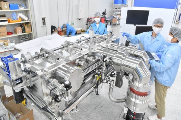
‘EMiLE’ system that is currently being developed does not reduce and carry out photolithography process on a circuit that is printed on a EUV mask just like current EUV lithography system. Instead, it applies ‘interference phenomenon’ through EUV light and evaluates the performance of a photoresist.
This system removes 11 mirrors that reflect EUV radiation and photomasks that are attached to an EUV lithography system and places a metallic part between a wafer and EUV light source.
The metallic part has two square holes that are spaced out regularly to the left and to the right. These square holes have 32nm metallic lines arranged uniformly and finely. This is called ‘grating’ that causes light diffraction phenomenon.
When EUV light source passes through two holes and comes to grating, light is diffracted and curved in many directions. Light that passes through these holes starts to interfere each other. During interference, there is a part where the intensity of light becomes stronger and there is also a part where the intensity becomes weaker. The part where the intensity of light becomes stronger touches EUV photoresist and forms a pattern that consists of 16nm vertical lines.
This system applies a characteristic of lithography process that prints patterns with light and checks the performance on how well photoresist patterns are formed.
ESOL also finished applying for necessary patterns regarding the system. Vice-President Lee Dong-geun of ESOL is confident that companies can now test EUV photoresists without having to purchase expensive EUV lithography system.
“EMiLE system’s cost is about 10% of the cost of current EUV lithography system.” said Vice-President Lee. “South Korean companies can now drastically increase opportunities to test the performance of an EUV photoresist and accelerate the development of EUV photoresists in a short period of time.”
ESOL is almost finished with developing EUV mask review system that uses ‘zone plate lens’. This system can check whether an EUV mask is defective or not at a relatively low cost.
“If our semiconductor systems are utilized for semiconductor testbeds that will be set up in the future, companies will be able to reduce disparity in technology with Japanese photoresist manufacturers.” said CEO Kim Byung-guk of ESOL. “We are also developing EUV photoresist sensitivity grading system that is much cheaper than current EUV photoresist sensitivity grading system on the market.”
Staff Reporter Kang, Hyeryung | kang@etnews.com