Experts who saw Japanese Government’s regulation on photoresist all agree that Japanese Government made a careful plan to target South Korean industries. They believe that this measure can suffocate R&D and have negative impact on entire manufacturing process of semiconductors. Japanese Government’s sanction selects only items that will target South Korean semiconductor industry and not items that can be replaced or already localized in South Korea.
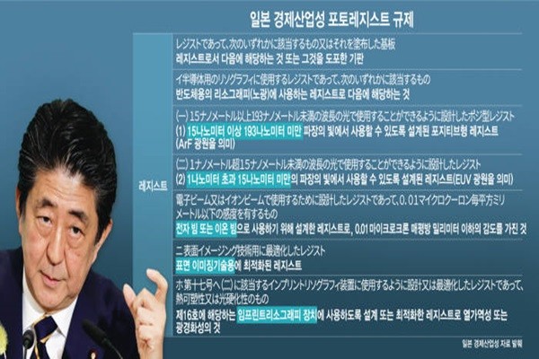
Ministry of Economy, Trade and Industry (METI) of Japanese Government regulates four types of photoresists and they are positive resist that is used in wavelength between 15 nm and 193nm, resist that is used in wavelength between 1nm and 15nm, resist for electronic beam or ion beam, and resist used for imprint lithography device.
Photoresist is an important material used for photolithography process that is one of major semiconductor processes. Photolithography indicates a process of printing rough sketch of a circuit onto a wafer using light. A circuit is drawn on top of a wafer by applying photoresist on top of a wafer and shooting light. Photoresist is a material that is absolutely needed during semiconductor processing.
Photolithography process differs based on wavelength of light. Shorter wavelength indicates production of more precise semiconductors. Different photoresists are also used depending on wavelength.
Experts analyzed that ‘15nm to 193nm resist’ indicates a semiconductor resist that uses ArF (Argon Fluoride) light source. Also, they interpreted that ‘1nm to 15nm resist’ indicates a photoresist used for EUV (Extreme Ultraviolet).
“Wavelengths of ArF light source and EUV light source that are used by Samsung Electronics and SK Hynix to manufacture high-end semiconductors are 193nm and 13.5nm respectively.” said Professor Ahn Jin-ho of Hanyang University. “It can be seen that Japanese Government practically blocked off exportation of photoresists by setting up range of wavelengths.”
Professor Ahn is saying that Japanese Government targeted semiconductor materials that are currently used by Samsung Electronics and SK Hynix. Semiconductor resist using EUV light source especially is an important material for Samsung Electronics to grow its system semiconductor business including foundry.
Samsung Electronics is currently obtaining orders from global IT businesses such as NVIDIA and Qualcomm through its EUV technology. However, Japanese Government did not miss this opportunity and placed photoresist for EUV on its list of photoresists subject to regulation.
KrF (Krypton Fluoride) light source with 248nm wavelength is also used during photolithography process. KrF light source is the previous generation of ArF light source and it is excluded from Japanese Government’s regulatory list. KrF photoresist is already localized in South Korea and it will be unnecessary for Japanese Government to regulate it if it wants to pressure South Korean Government.
“South Korean businesses such as Dongjin Semichem can supply KrF photoresists to Samsung Electronics.” said Professor Ahn. “Japanese Government only picked ones that can have the most impact on our semiconductor industry.”
Another problem is that Japanese Government decided to regulate exportation of photoresists for R&D on next-generation products.
Electronic beam and ion beam are beams that are used during manufacturing process of a mask. Although they are not commercialized for photolithography purpose, they are seen as next-generation light sources that can implement super-fine circuits through wavelengths that are shorter than EUV.
‘Imprint lithography’ is a photolithography process that prints nano-patterns that are already imprinted on top of a wafer and it is seen as a photolithography process for the future.
“Japanese Government’s regulation blocks every photoresist that is being invested by South Korean businesses, universities, and research institutes when Japanese businesses are closely working with our businesses to research and develop next-generation technologies.” said Professor Kwon Ki-cheong of Kwangwoon University.
It is heard that semiconductor device manufacturers are in a dire situation as they do not have replacements for photoresists. “Our inventory will only about a month and amount of inventories that we bring in now will be limited as they have effective dates.” said a representative for the industry.
Experts state that aftereffects must be minimized in order to deal with this current situation.
“Although some materials are localized, it will take at least five years to completely replace photoresists that are regulated by Japanese Government.” said one expert from the industry. “Since this issue occurred due to a diplomatic problem, it is more up to South Korean Government rather than businesses to quickly resolve this issue.”
Staff Reporter Yun, Geonil | benyun@etnews.com & Staff Reporter Kang, Hyeryung | kang@etnews.com