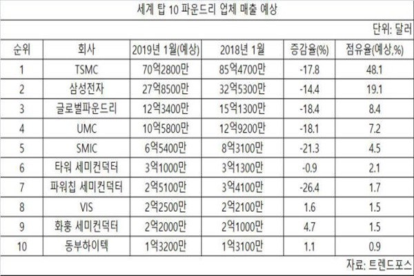
Samsung Electronics took a direct hit from TSMC in 2015 when it lost entire supply of APs (Application Processor) for Apple to TSMC that came out with FO-WLP (Fan Out-Wafer Level Package) technology. Initially, iPhones’ APs were produced by both TSMC and Samsung Electronics. However, TSMC turned the tables by commercializing FO-WLP technology for the first time in the world and it has earned entire supply of APs until 2020.
As a result, Samsung Electronics was in total state of emergency. It was a costly mistake for overlooking importance of semiconductor packaging technology. Packaging is a process that packages silicon wafer chips (die) that are manufactured and it protects them from outside moisture, impurity, and impact and allows them to transfer signals with main PCB (Printed Circuit Board). It was relatively not interested in back-end process of semiconductor manufacturing process and it found out later that back-end process was an important element that defines performance of a semiconductor.
Samsung Electronics formed a task force to start taking necessary actions. It cooperated with Samsung Electro-Mechanics to start developing FO-PLP (Fan Out- Panel Level Package) technology. FO-PLP technology brings out I/O connection wiring outside of a semiconductor chip (die) to increase performance of a semiconductor and it reduces production cost by not using a board. FO-PLP especially uses a rectangular panel that allows for higher productivity than FO-WLP.
Samsung Electro-Mechanics succeeded in commercializing FO-PLP technology. It packaged APs that were used for Samsung Electronics’ ‘Galaxy Watches’ in 2018 through FO-PLP technology. Although there have been visual results, it seems that FO-PLP technology lacks in many areas. Samsung Electro-Mechanics lacks technical skill that can package Smartphone AP, which is a high-performance semiconductor, and production capacity to produce tens of millions of APs annually. At the moment, Samsung Electro-Mechanics’ PLP is only applied to an AP of a Smart Watch and is not applied to an AP of a Smartphone yet. It also has only one PLP production line.

It seems that a need for investments for continuous R&D and large-scale facilities and equipment and a need for packaging technology to raise Samsung Electronics’ competitive edge in foundry are the reasons why there is a business transaction between Samsung Electro-Mechanics and Samsung Electronics. Industries believe that Samsung Electronics will be in charge of this project instead of Samsung Electro-Mechanics to quickly raise level of relevant technologies and mass-production ability to bring back Apple’s orders in 2021 when the monopolistic contract between Apple and TSMC ends.
“Samsung Electronics needs to show Apple in 2020 that it has all necessary preparations if it wants to win back Apple’s orders in 2021.” said a representative for the semiconductor packaging industry. “Samsung Electronics and Samsung Electro-Mechanics has come to an agreement as they believe that it is necessary for them to carry out facilities and equipment investments on full-scale this year and to build their references.”
It is likely that Samsung Electronics will strengthen its competitive edge in semiconductor packaging by acquiring PLP technology from Samsung Electro-Mechanics. It is expected that Samsung Electronics will look to create synergy by adding packaging technology to its development of fine foundry processes (7nm and 5nm).
Samsung Electronics is also working on development of FO-WLP technology. FO-PLP is a project that was pushed by Chairman Kwon Oh-hyeon while he was working as the vice-chairman, and FO-WLP has been started under Vice-Chairman Kim Ki-nam’s order.
Samsung Electro-Mechanics will be able to improve its financial structure by selling PLP business that had been in deficit. However, it needs to find a new driving force as the result of selling PLP business. PLP had been a project that was under direct leadership of CEO of Samsung Electro-Mechanics.
When Samsung Electronics starts investments into semiconductor packaging technologies on full-scale, there will be positive impact on semiconductor packaging industries such as FO-PLP or FO-WLP. Increase in level of importance of semiconductor packaging can lead to vitalization of relevant industries. NEPES from South Korea currently has next-generation packaging technologies such as FO-PLP and FO-WLP.
It will be interesting to see whether Samsung Electronics will be able to win back Apple’s orders and expand its foundry and non-memory businesses by strengthening its competitive edge in packaging.
Staff Reporter Yun, Geonil | benyun@etnews.com